#atomiclayer نتائج البحث

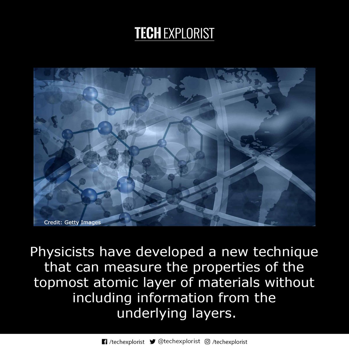
Physicists find a new way to measure the properties of a material’s surface layer. #atomiclayer #physicists #properties #propertiesofmaterials #science #techexplorist

We are looking forward to a three-day meeting dedicated to the #science and #technology of #atomiclayer controlled deposition of #thinfilms and now topics related to #atomiclayeretching. We hope to see you there!

A Cheaper way to Scale up Atomic Layer Deposition powersystemsdesign.com/articles/a-che… @EPFL #epfl #atomiclayer #atomic #psd

Rui Zhang #PhD @IMNS_UoE is presenting his #atomiclayer process work at #EIPBN 2017 Conference - research in collaboration with @memsstar_


#ALDALE2018 is one of the most important conferences in #atomiclayer processing. #LamResearch is excited to present on some of the latest atomic layer #etch #innovations. Check out our latest blog for the schedule: bit.ly/2NDFaUf #chip #semiconductorindustry

We'll be at the EFDS European Research Association for Thin Layers online event this March - join us at this event to discuss atomic layer deposition simulations at the atomic scale with #QuantumATK bit.ly/2OGsoKz #thinfilms #atomiclayer

Connect with Umberto Martinez at the EFDS European Research Association for Thin Layers online event today - join us at this event to discuss atomic layer deposition simulations at the atomic scale with #QuantumATK bit.ly/2OGsoKz #atomiclayer #thinfilms


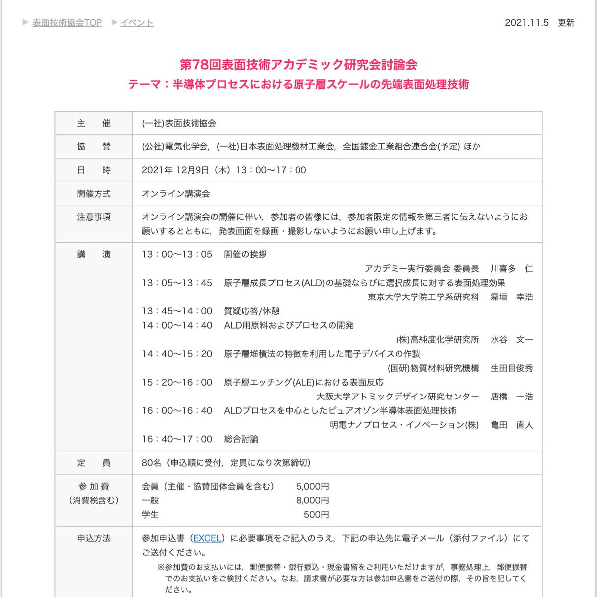
12月9日(木)13:00-17:00に、表面技術協会が第78回表面技術アカデミック研究会討論会をオンライン開催。テーマは『半導体プロセスにおける原子層スケールの先端表面処理技術』。講演5件と総合討論。詳細は bit.ly/3EMbH57 に。 #seminar #semiconductor #AtomicLayer #SurfaceFinishing

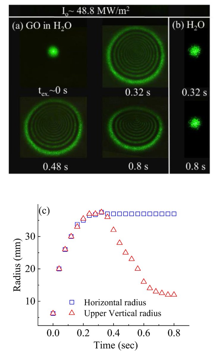
#Highly_cited "Spatial Self-Phase Modulation in Graphene-Oxide Monolayer" by Tikaram Neupane et al. 👉You can read it here: mdpi.com/2073-4352/13/2… #graphene #AtomicLayer

Jobs in San Jose: MECHANICAL ENGINEER SR (San Jose, CA) http://goo.gl/fb/sodmX #craigslist #atomiclayer

From the MRS Bulletin: The phase transformation was discovered serendipitously. #MaterialsScience #AtomicLayer #SnS2 #SnS @Tianyuliu_Chem cambridge.org/core/services/…


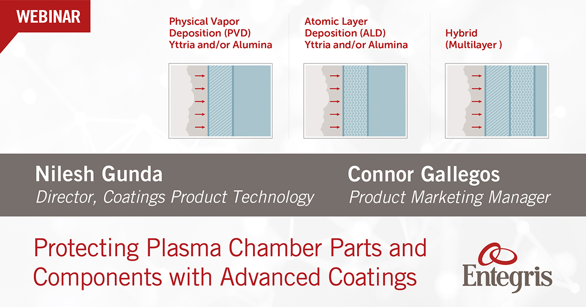
Join Connor Gallegos, Product Mgr. & Nilesh Gunda, Dir. Coatings Product Technology in this webinar as they share the importance of #advancedcoatings for chamber parts & components & 3 successful coating methods. hubs.ly/H0q96v10. #atomiclayer #semiconductor #chemicalvapor

C news : youtu.be/0fbQX5VJmew #carbonatoms #consist #atomiclayer #proprerietes #extremly #flexibility #hexagonaly ;-)

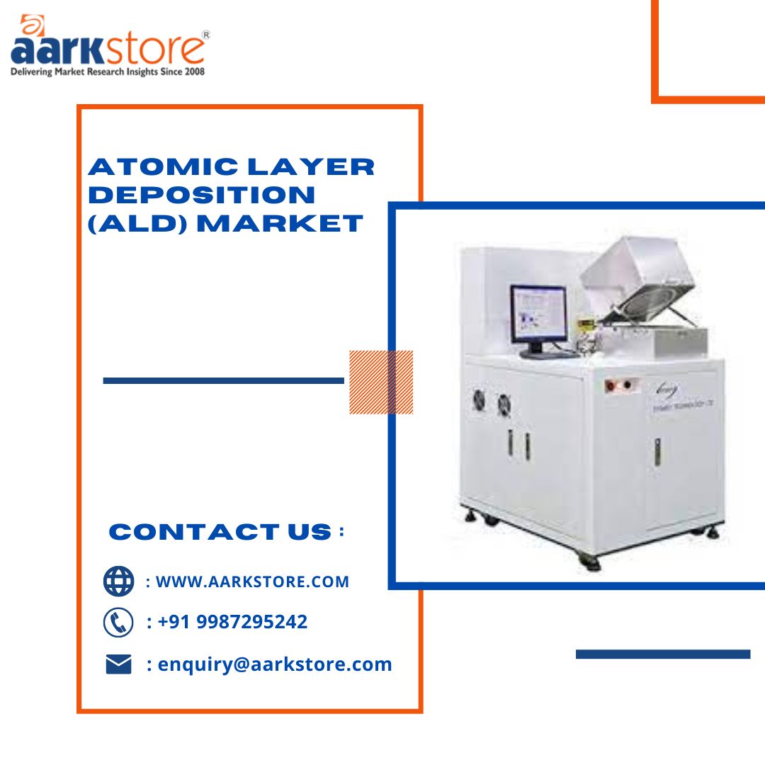
the global #atomiclayer #deposition market is set to achieve an incremental growth of USD 1.7 billion, accelerating at a CAGR of almost 6.7%. VISIT - bit.ly/3V3KVgn #swot #swotanalysis #marketresearch #aarkstore #depositionmarket #ALD #atomiclayerdeposition

From the MRS Bulletin: The phase transformation was discovered serendipitously. #MaterialsScience #AtomicLayer #SnS2 #SnS @Tianyuliu_Chem qoo.ly/378xwt

Nokia Obtains Graphene Grant goo.gl/fb/YxVAa #geekygadgets #100x #atomiclayer #billions #cleanwater #corrosion
We are extremely proud to announce our collaboration with #ESABIC to further advance the development of ATLANT 3D Nanofabricator™ 0G systems, the first-ever selective area direct write #atomiclayer #zerogravity #R&D unit for #Space and Beyond🌍🤝 eu1.hubs.ly/y0yw490

#perovskitesolarcell based on #atomiclayer architecture bit.ly/2gZoAlc


Atomic-Layer IrOx Enabling Ligand Effect Boosts Water Oxidation Electrocatalysis | Journal of the American Chemical Society #AtomicLayer #Ligand #Water #Oxidation #Electrocatalysis pubs.acs.org/doi/10.1021/ja…
pubs.acs.org
Atomic-Layer IrOx Enabling Ligand Effect Boosts Water Oxidation Electrocatalysis
An in situ formed IrOx (x ≤ 2) layer driven by anodic bias serves as the essential active site of Ir-based materials for oxygen evolution reaction (OER) electrocatalysis. Once being confined to...
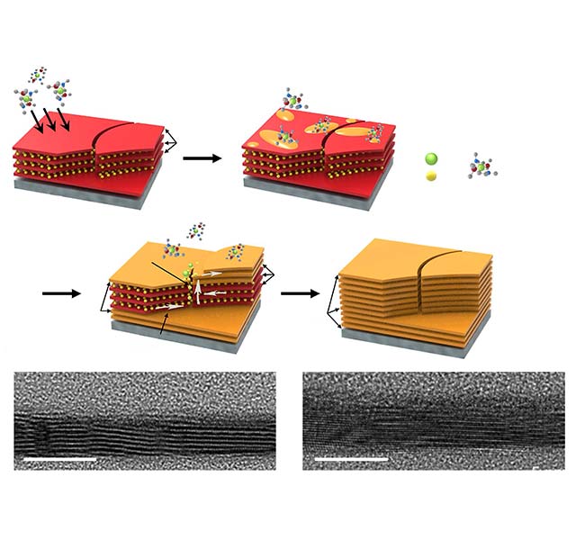
Colloidal Atomic Layer Deposition on Nanocrystals Using Ligand-Modified Precursors | Journal of the American Chemical Society @lnce_epfl @EPFL_CHEM_Tweet @EPFL_en #Colloidal #AtomicLAyer #Deposition #Nanocrystals #LigandModified #Precursors pubs.acs.org/doi/10.1021/ja…
#Highly_cited "Spatial Self-Phase Modulation in Graphene-Oxide Monolayer" by Tikaram Neupane et al. 👉You can read it here: mdpi.com/2073-4352/13/2… #graphene #AtomicLayer
the global #atomiclayer #deposition market is set to achieve an incremental growth of USD 1.7 billion, accelerating at a CAGR of almost 6.7%. VISIT - bit.ly/3V3KVgn #swot #swotanalysis #marketresearch #aarkstore #depositionmarket #ALD #atomiclayerdeposition
Physicists find a new way to measure the properties of a material’s surface layer. #atomiclayer #physicists #properties #propertiesofmaterials #science #techexplorist
We are looking forward to a three-day meeting dedicated to the #science and #technology of #atomiclayer controlled deposition of #thinfilms and now topics related to #atomiclayeretching. We hope to see you there!
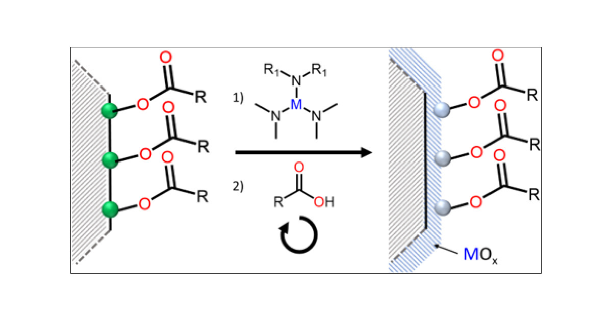
Elucidating the Reaction Mechanism of Atomic Layer Deposition of Al2O3 with a Series of Al(CH3)xCl3–x and Al(CyH2y+1)3 Precursors @Stanford #Mechanism #AtomicLayer #Deposition #Al2O3 pubs.acs.org/doi/10.1021/ja…
pubs.acs.org
Elucidating the Reaction Mechanism of Atomic Layer Deposition of Al2O3 with a Series of Al(CH3)xC...
The adsorption of metalorganic and metal halide precursors on the SiO2 surface plays an essential role in thin-film deposition processes such as atomic layer deposition (ALD). In the case of aluminum...
#Fractilia’s CTO Chris Mack weighs in on new developments in advanced etch processing for next-gen #semiconductors in this @SemiEngineering article by @MarkLaPedus bit.ly/3v1inu6 #EUV #AtomicLayer#Etch #GateAllAround #3DNAND
semiengineering.com
Highly Selective Etch Rolls Out For Next-Gen Chips
Manufacturing 3D structures will require atomic-level control of what's removed and what stays on a wafer.
We are extremely proud to announce our collaboration with #ESABIC to further advance the development of ATLANT 3D Nanofabricator™ 0G systems, the first-ever selective area direct write #atomiclayer #zerogravity #R&D unit for #Space and Beyond🌍🤝 eu1.hubs.ly/y0yw490
12月9日(木)13:00-17:00に、表面技術協会が第78回表面技術アカデミック研究会討論会をオンライン開催。テーマは『半導体プロセスにおける原子層スケールの先端表面処理技術』。講演5件と総合討論。詳細は bit.ly/3EMbH57 に。 #seminar #semiconductor #AtomicLayer #SurfaceFinishing
#US-Made #Batteries Enhanced With #AtomicLayer #Deposition @ForgeNano #urjadaily #SolarNews #solarenergy #Battery urjadaily.com/us-made-batter…
Connect with Umberto Martinez at the EFDS European Research Association for Thin Layers online event today - join us at this event to discuss atomic layer deposition simulations at the atomic scale with #QuantumATK bit.ly/2OGsoKz #atomiclayer #thinfilms
We'll be at the EFDS European Research Association for Thin Layers online event this March - join us at this event to discuss atomic layer deposition simulations at the atomic scale with #QuantumATK bit.ly/2OGsoKz #thinfilms #atomiclayer

Do you want to achieve atomic-scale precision for etching, deposition and 1D & 2D materials growth? Find out more about our fabrication solutions: okt.to/HqM4ad #plasmatechnology #atomicscale #atomiclayer
From the MRS Bulletin: The phase transformation was discovered serendipitously. #MaterialsScience #AtomicLayer #SnS2 #SnS @Tianyuliu_Chem cambridge.org/core/services/…
From the MRS Bulletin: The phase transformation was discovered serendipitously. #MaterialsScience #AtomicLayer #SnS2 #SnS @Tianyuliu_Chem qoo.ly/378xwt

12月9日(木)13:00-17:00に、表面技術協会が第78回表面技術アカデミック研究会討論会をオンライン開催。テーマは『半導体プロセスにおける原子層スケールの先端表面処理技術』。講演5件と総合討論。詳細は bit.ly/3EMbH57 に。 #seminar #semiconductor #AtomicLayer #SurfaceFinishing
Physicists find a new way to measure the properties of a material’s surface layer. #atomiclayer #physicists #properties #propertiesofmaterials #science #techexplorist
A Cheaper way to Scale up Atomic Layer Deposition powersystemsdesign.com/articles/a-che… @EPFL #epfl #atomiclayer #atomic #psd
We are looking forward to a three-day meeting dedicated to the #science and #technology of #atomiclayer controlled deposition of #thinfilms and now topics related to #atomiclayeretching. We hope to see you there!
From the MRS Bulletin: The phase transformation was discovered serendipitously. #MaterialsScience #AtomicLayer #SnS2 #SnS @Tianyuliu_Chem cambridge.org/core/services/…
Rui Zhang #PhD @IMNS_UoE is presenting his #atomiclayer process work at #EIPBN 2017 Conference - research in collaboration with @memsstar_
#ALDALE2018 is one of the most important conferences in #atomiclayer processing. #LamResearch is excited to present on some of the latest atomic layer #etch #innovations. Check out our latest blog for the schedule: bit.ly/2NDFaUf #chip #semiconductorindustry
We'll be at the EFDS European Research Association for Thin Layers online event this March - join us at this event to discuss atomic layer deposition simulations at the atomic scale with #QuantumATK bit.ly/2OGsoKz #thinfilms #atomiclayer
Connect with Umberto Martinez at the EFDS European Research Association for Thin Layers online event today - join us at this event to discuss atomic layer deposition simulations at the atomic scale with #QuantumATK bit.ly/2OGsoKz #atomiclayer #thinfilms
#Highly_cited "Spatial Self-Phase Modulation in Graphene-Oxide Monolayer" by Tikaram Neupane et al. 👉You can read it here: mdpi.com/2073-4352/13/2… #graphene #AtomicLayer
From the MRS Bulletin: The phase transformation was discovered serendipitously. #MaterialsScience #AtomicLayer #SnS2 #SnS @Tianyuliu_Chem qoo.ly/378xwt
Join Connor Gallegos, Product Mgr. & Nilesh Gunda, Dir. Coatings Product Technology in this webinar as they share the importance of #advancedcoatings for chamber parts & components & 3 successful coating methods. hubs.ly/H0q96v10. #atomiclayer #semiconductor #chemicalvapor
the global #atomiclayer #deposition market is set to achieve an incremental growth of USD 1.7 billion, accelerating at a CAGR of almost 6.7%. VISIT - bit.ly/3V3KVgn #swot #swotanalysis #marketresearch #aarkstore #depositionmarket #ALD #atomiclayerdeposition
Something went wrong.
Something went wrong.
United States Trends
- 1. Lakers 49.3K posts
- 2. Dillon Brooks 6,351 posts
- 3. Giants 83.9K posts
- 4. Bron 23.9K posts
- 5. #WWERaw 68.7K posts
- 6. Patriots 127K posts
- 7. Drake Maye 23.8K posts
- 8. Dart 35.5K posts
- 9. Suns 18.2K posts
- 10. Collin Gillespie 1,923 posts
- 11. Diaz 33.6K posts
- 12. Devin Williams 7,607 posts
- 13. Ryan Nembhard 3,856 posts
- 14. Gunther 14.7K posts
- 15. Pats 15.9K posts
- 16. #AvatarFireAndAsh 2,542 posts
- 17. Joe Schoen 3,389 posts
- 18. Devin Booker 2,535 posts
- 19. STEAK 10.3K posts
- 20. Younghoe Koo 6,716 posts