You might like


#P1206 Aluminium deposited on batch, and process on hold for easter hollidays
#P1206 ALD Al2O3 deposited on extremely thin SiO2 as gate dielectrics, trial on one wafer.
#P1206 wafers came back from IBS. Next step is final gate oxidation & polysilicon deposition.
#P1206 wafers are ready to be sent to IBS for the second channel implantation.
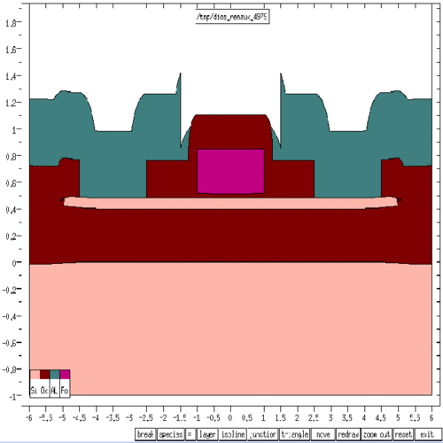
#P1206 LOCOS isolation performed on all wafers with two recipes for comparaison
New CMOS process #P1206 started in June...(never too late to let you know :) )
Asked if there were significant differences between finfet transistors and fully depleted SOI transistors - the... fb.me/1kfUeE5MU
#P1103 Great news,the UCL CMOS SOI is back on tracks. Threshold voltage are again back to normal values.... :-D
#P1103 Contact Pad opening...process will be terminated on Monday 14/11


United States Trends
- 1. #GMMTV2026 2.28M posts
- 2. Good Tuesday 27.7K posts
- 3. MILKLOVE BORN TO SHINE 377K posts
- 4. #tuesdayvibe 1,997 posts
- 5. WILLIAMEST MAGIC VIBES 53.7K posts
- 6. Chelsea 212K posts
- 7. MAGIC VIBES WITH JIMMYSEA 56.4K posts
- 8. Mark Kelly 211K posts
- 9. #JoongDunk 85.1K posts
- 10. Barcelona 158K posts
- 11. Alan Dershowitz 3,218 posts
- 12. TOP CALL 9,221 posts
- 13. #ONEPIECE1167 8,249 posts
- 14. Jim Croce N/A
- 15. AI Alert 8,074 posts
- 16. Barca 81.6K posts
- 17. Unforgiven 1,162 posts
- 18. Maddow 14.9K posts
- 19. Benedict Arnold 7,407 posts
- 20. Check Analyze 2,509 posts
You might like
-
 Sam Zeloof
@szeloof -
 ASML
ASML
@ASMLcompany -
 SemiWiki
@DanielNenni -
 ZEISS Group
@ZEISS_Group -
 EL_gringo 🇧🇪🇺🇦🇪🇺
@Kortak -
 Cadence
@Cadence -
 Optica
@OpticaWorldwide -
 Marvell Technology
@MarvellTech -
 GlobalFoundries
@GlobalFoundries -
 ieee iedm
@ieee_iedm -
 Tech Briefs
@TechBriefsMag -
 SOl & Engineered Substrates
@soiconsortium -
 Ed Sperling
@Chip_Insider -
 HiPEAC
@hipeac -
 Brewer Science
@brewerscience
Something went wrong.
Something went wrong.