
You might like


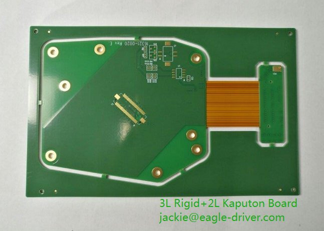
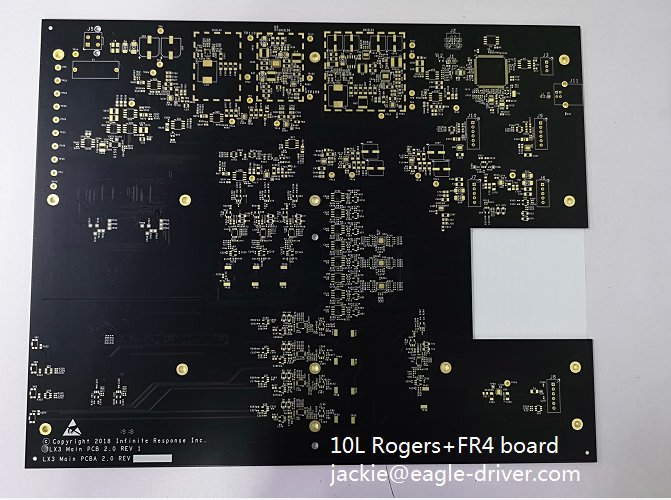
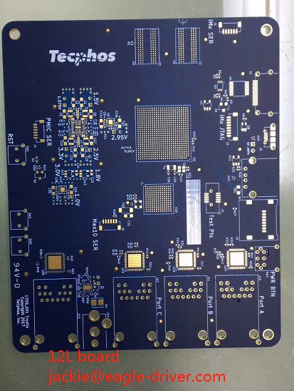
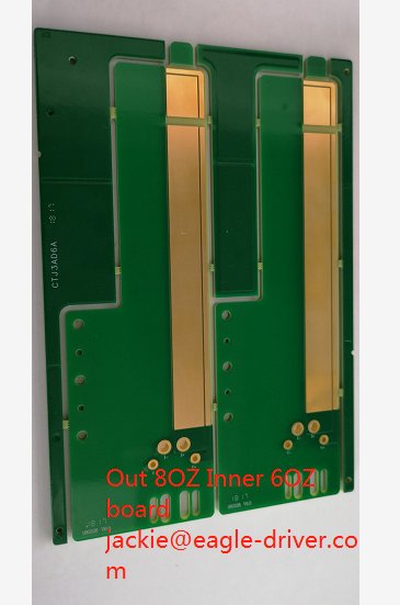
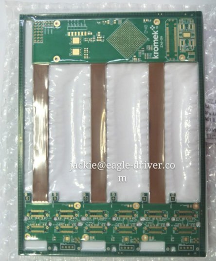
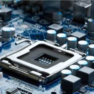
这是我们--EAGLE DRIVER ELECTRONIC LIMITED,制作PCB的能力!18L HDI + 8L刚性+ 2L刚性+ 4L Flex
@ Acromag jackie from china Eagle Driver PCB,providing 1-50 layers PCB,High quality: Blind/Buried Hole Board, High Tg Thick Copper PCB, Mix- Material Multilayer PCB, Flexi-rigid Board, Flexible Board, Metal Core Board...Skype and E-mail:[email protected]
@ AitechDefense Hi, I'm jackie.We had a chat before.PCB cooperation is possible.My other account was restricted by linkedin.This is my new number.Please add it.Thank you very much!
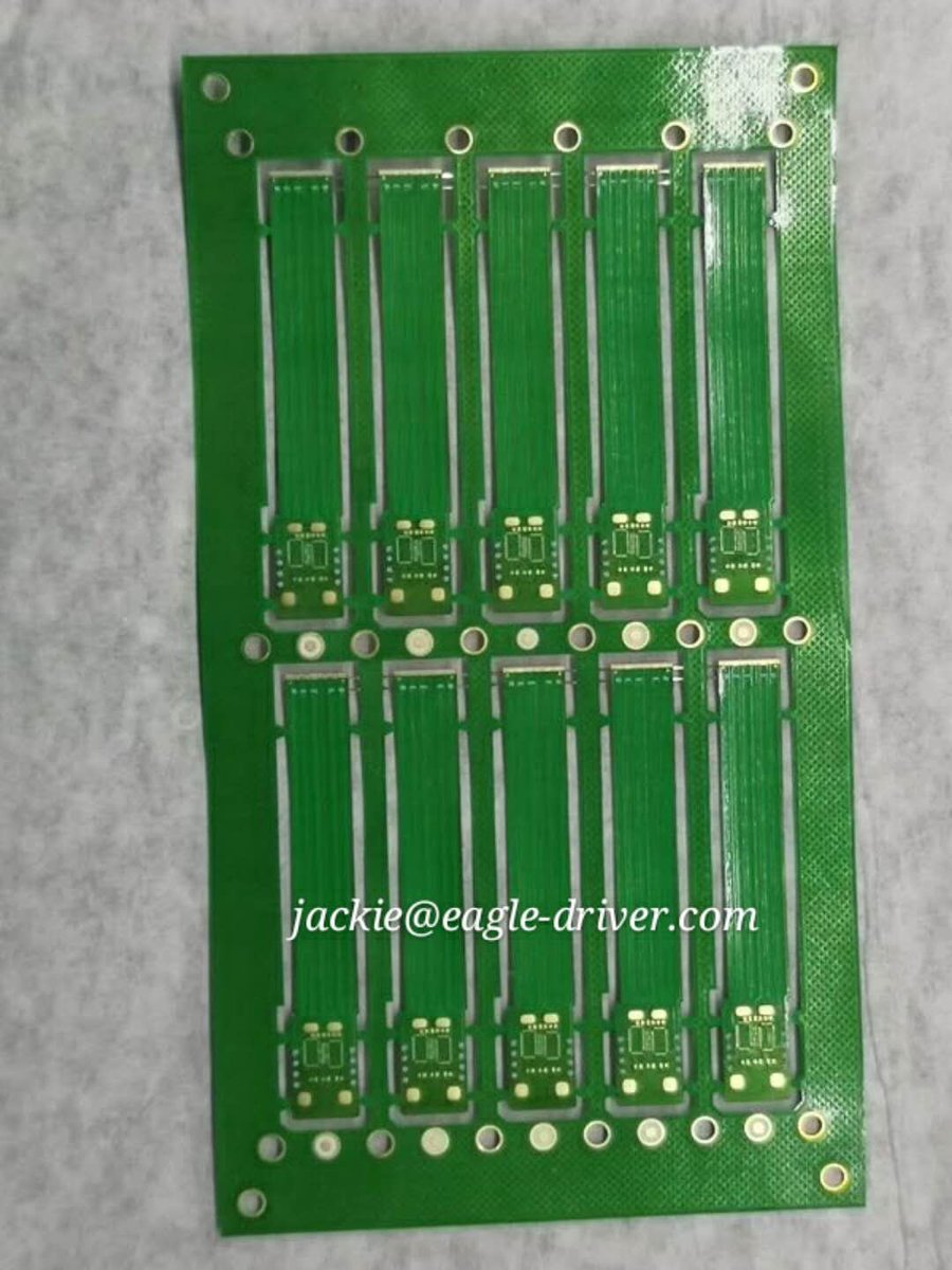
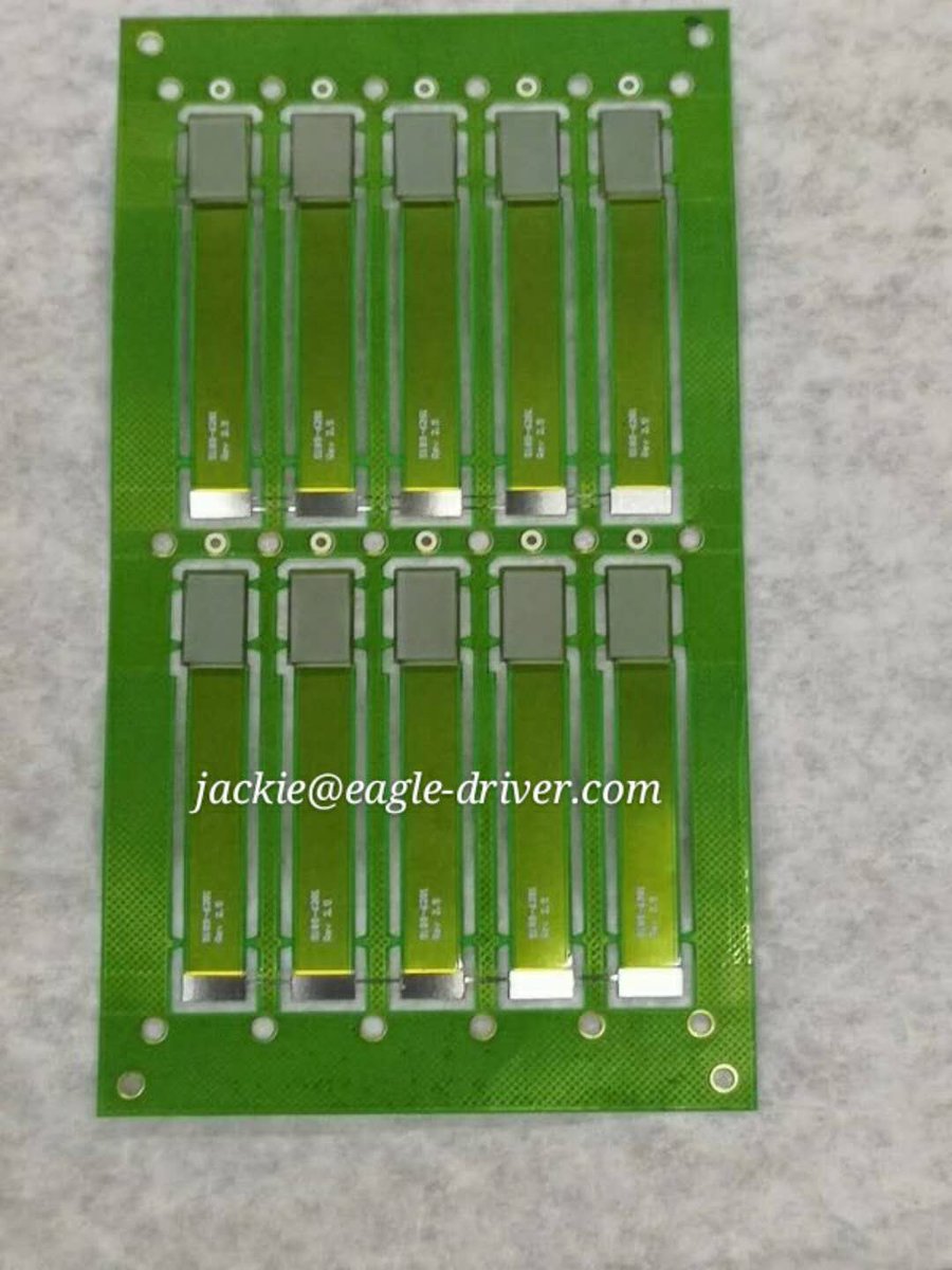
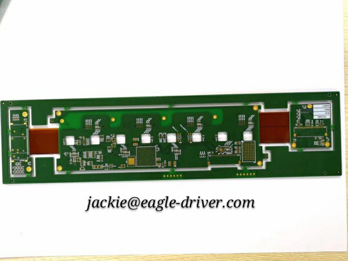
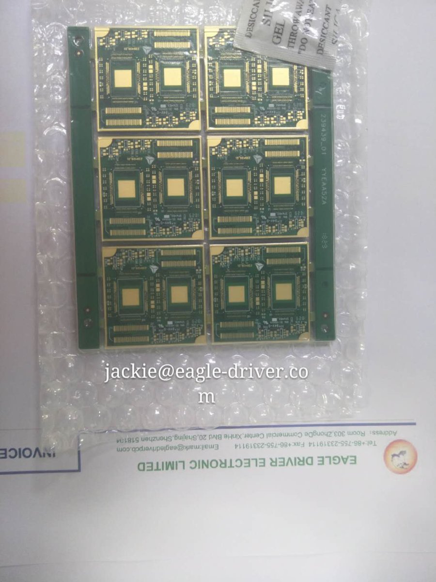
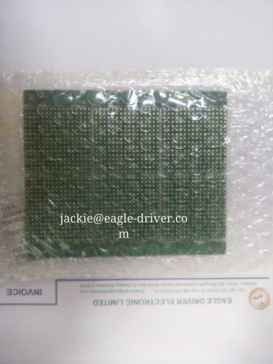
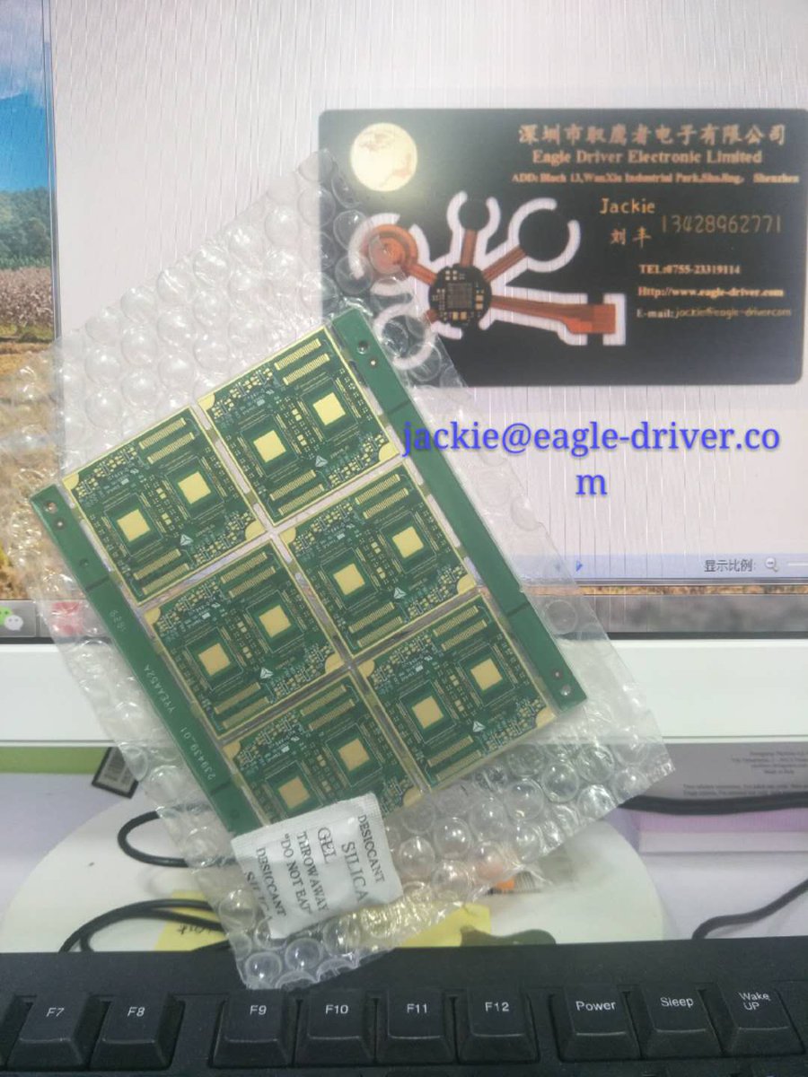
高难度PCB专用PCB--大型套装 生产困难的PCB,特殊的PCB。对我们来说,这是一门艺术,它是一个挑战,它是一项成就。我是EAGLE DRIVER ELECTRONIC LIMITED,PCB生产战斗机。 eagledriver166823352.wordpress.com/2018/08/21/hig…
High difficulty PCB special PCB-- large set issuu.com/jackieliu5/doc… via @Issuu
Analysis and method of plate deformation in PCB process issuu.com/jackieliu5/doc… via @Issuu


Power supply design,FPC design experience issuu.com/jackieliu5/doc… via @Issuu
高频PCB设计实用技巧摘要 PCB设计得更小,更快,更便宜。由于互连点是电路链中最薄弱的环节,在射频设计中, eagledriver166823352.wordpress.com/2018/08/08/sum…


Summary of practical tips for high frequency PCB design issuu.com/jackieliu5/doc… via @Issuu
5G era -- opportunity for PCB industry to take off again 5G - has become a buzzword of the age.The main goal of 5G networks is to keep end users connected all the time.The devices are far more than just smartphones. eagledriver166823352.wordpress.com/2018/08/06/5g-…
5G era -- opportunity for PCB industry to take off again issuu.com/jackieliu5/doc… via @Issuu
Practical summary of high frequency PCB design The PCB is designed to be smaller, faster and cheaper.As the interconnection point is the weakest link in the circuit chain, eagledriver166823352.wordpress.com/2018/08/02/pra…
Practical summary of high frequency PCB design issuu.com/jackieliu5/doc… via @Issuu
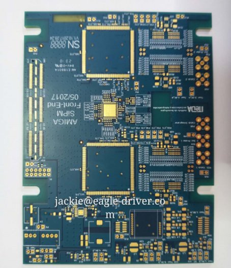
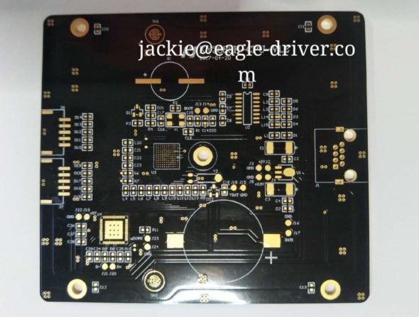
再次带来一个困难的PCB 经过这么多年,最令人满意的是制造另一个困难的PCB。 参数:10层,3阶HDI,镍钯金,树脂塞孔,阻抗板,板厚3.0 在这些年里,最激动人心的是有一块无法制造的PCB。 前天,我收到了一个4层板,但我无法接受订单原因:必须是10uM的的的(400U)0.01毫米的黄金。
Bring a difficult PCB again issuu.com/jackieliu5/doc… via @Issuu
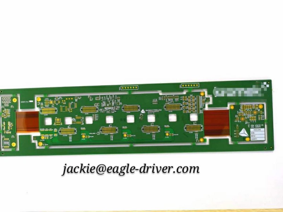
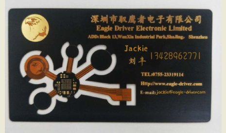
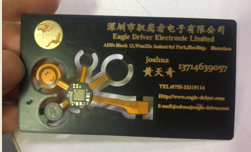
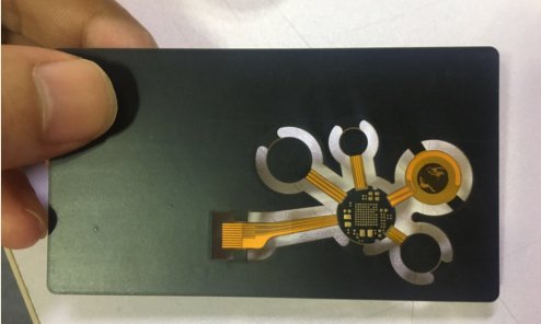
See our PCB gold card, know what we do We are professional in PCB production. You can see from our business card that the four layers of hard and soft are combined and the surface is heavy gold.There's no feeling of being tall.This is the legend of the gilded business card.


United States Trends
- 1. Sonny Gray 1,300 posts
- 2. #GMMTV2026 4.16M posts
- 3. Thankful 49.9K posts
- 4. #csm221 2,454 posts
- 5. #OurCosmicClue_Wooyoung 24.3K posts
- 6. Gone in 60 1,101 posts
- 7. National Treasure 3,759 posts
- 8. Happy Thanksgiving 18.4K posts
- 9. Mark Kelly 249K posts
- 10. Mainz Biomed N/A
- 11. MILKLOVE BORN TO SHINE 712K posts
- 12. Hegseth 119K posts
- 13. #LUNÉSelcaDay 2,749 posts
- 14. #YouManiacSeries 102K posts
- 15. Good Tuesday 39.4K posts
- 16. Ghost Rider 1,284 posts
- 17. Lord of War N/A
- 18. Raising Arizona N/A
- 19. Alan Dershowitz 5,425 posts
- 20. Taco Tuesday 14.3K posts


Something went wrong.
Something went wrong.