
Ray Ming
@raypcb3
Our products are widely used in power supplies, computers, communications, optoelectronics, industrial instruments, automobile and other consumer electronics.
You might like


Immersion gold Purple + Hasl Lead Free Black, 2MM Thickness, 4 Layer, 1OZ Finished copper goo.gl/DYa1Au


Double-sided HASL Finished, Material:FR-4, Finished Thinkness: 1.6mm, Surface Finishing: HASL goo.gl/Wkg9Re


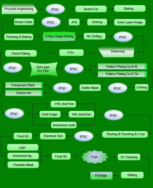


PCB is a well known term in the electronic industry. Basically it consists of several layers..goo.gl/uNpNnS


For a common understanding, several layers of insulating materials combined with electrical.. goo.gl/QOBubi


6 layers+Impedance PCB, Item:2848, Details: 6 layers+Impedance, Solder resist:LPI Dark blue goo.gl/DwzbHZ


United States Trends
- 1. #AEWDynamite 42K posts
- 2. Epstein 1.43M posts
- 3. #AEWBloodAndGuts 5,355 posts
- 4. #Survivor49 3,407 posts
- 5. Darby 5,027 posts
- 6. Kyle O'Reilly 1,213 posts
- 7. Steph 23.1K posts
- 8. Moxley 2,548 posts
- 9. Hobbs 28.8K posts
- 10. #SistasOnBET 2,149 posts
- 11. Skye Blue 4,021 posts
- 12. Caruso 3,777 posts
- 13. Paul Reed 2,032 posts
- 14. Warriors 47.4K posts
- 15. Draymond 8,604 posts
- 16. Mark Briscoe N/A
- 17. Claudio 24.9K posts
- 18. Knicks 34.3K posts
- 19. Thunder 41K posts
- 20. Hannah Hidalgo 4,604 posts


Loading...
Something went wrong.
Something went wrong.