
San Francisco Circuits
@sfcircuits
One-Stop PCB Manufacturing & Assembly - our specialty is delivering advanced prototypes from intricate layouts & advanced technologies.
You might like


🔒System integrators face unique challenges: protecting sensitive design data while delivering high-reliability PCBs. San Francisco Circuits supports secure R&D with NIST & CMMC-compliant manufacturing and rapid prototyping. Learn more: sfcircuits.com/system-integra…

⚙️Heavy copper PCBs use copper weights from 4 to 10 oz per square foot to boost current capacity and heat management. These boards power high-demand systems in defense, aerospace, and industrial electronics. Learn more about heavy copper boards here: sfcircuits.com/pcb-production…
Our new PCB Stackup Calculator lets you build and visualize stackups from 4 to 14 layers in just a few clicks. Start experimenting with your next design today: sfcircuits.com/pcb-stackup-ca…
sfcircuits.com
PCB Stackup Calculator / Design Tool - San Francisco Circuits
San Franciso Circuits PCB Stackup Calculator is a simple design tool to help you design and visualize your multilayer PCB stackup from 4 to 14 layers.
Check out our latest guide covering via types for multilayer circuit boards. Understand how different vias enable compact layouts and efficient signal routing. 🔗 Read the full guide: sfcircuits.com/pcb-school/pcb…
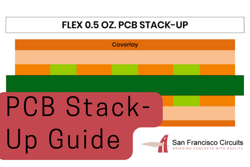
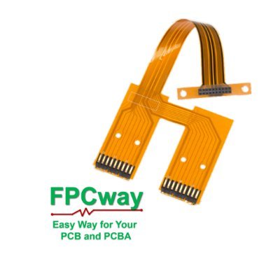
Check out our updated Flex PCB Capabilities page, covering: 💡 Ultra-thin flex (as slim as 12.5 microns) 📲 Streamlined designs without bulky wiring or connectors 🔗 Turn times, materials, layer stacks and more: sfcircuits.com/pcb-production…
🔩 Thru-hole technology ensures strong PCB connections and durability. When placing connectors or diodes, check orientation for reliable soldering. Mark the cathode on the silkscreen to avoid assembly errors.💡 Learn more: sfcircuits.com/pcb-school/pcb…
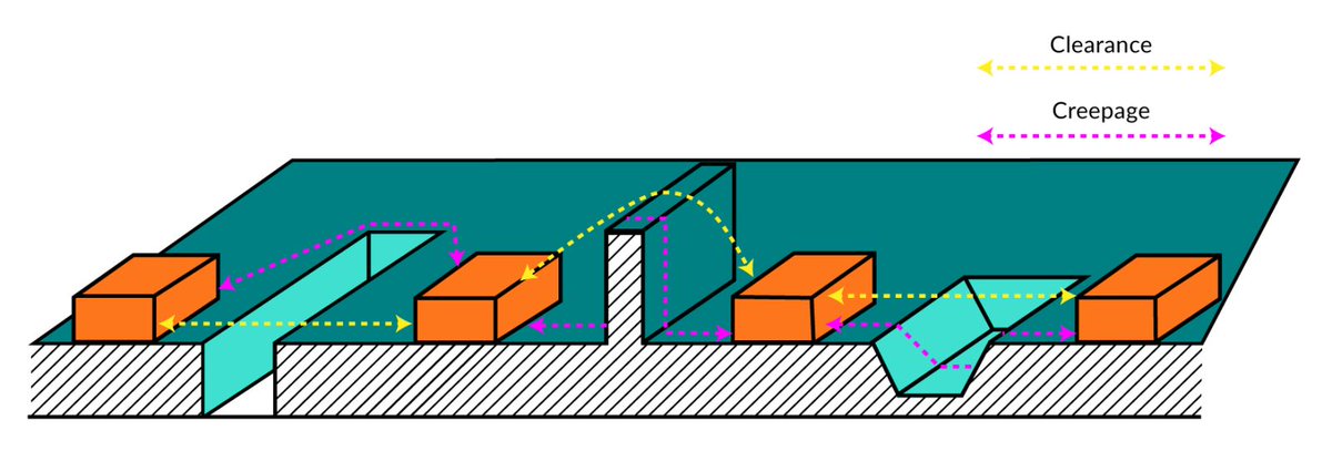
Our article on PCB line spacing, clearance, and creepage has been featured in the latest issue of PCD&F. In the article, we dive into the crucial aspects of clearance and creepage in PCB design, especially for high-voltage applications. pcdandf.com/pcdesign/index…


Our January edition is now available digital.pcea.net – check out this month's coverage on #PCBdesign #PCBtraces #DfM #DfA #electronicsassembly #stencilprinting #EDA #designcareers #AI #additivemanufacturing #PCBbuying #leanmanufacturing Brought to you by @PCEAssociation.

Explore High-Speed Circuit Design with tips for speeds from 1MHz to gigabit levels and advanced signal integrity techniques. Optimize your PCB layouts for I2C, PCIe, and Ethernet. Learn more: ow.ly/FUq650TjVQT

New! Just added to our PCB Material Reference Guide - a section on Flex materials: Differences between Flexible Polyimide, Rigid Polyimide, and FR4 Read it here: ow.ly/a3fJ50SM3Mt
New in PCB School: PCB Line Spacing: A Comprehensive Breakdown for High Voltage Applications. As PCBs become more complicated, more precise measurements and spacing are required. This article explains PCB line spacing, tracing, clearance, and creepage. ow.ly/f2Vx50SewOa

.@sfcircuits takes an in-depth look at Via Tenting, the practice of using a soldermask layer to cover the via holes on a Printed Circuit Board (PCB). Learn more: hubs.la/Q02mlPzj0 #circuitboard #engineering #tech #circuit

Tenting vias with a soldermask layer, or leaving them untented, has its own set of advantages & disadvantages that designers should consider for each project. Check out our new article on Via Tenting Principles in PCB design here: ow.ly/Hsqu50QCCMb #PCBdesign


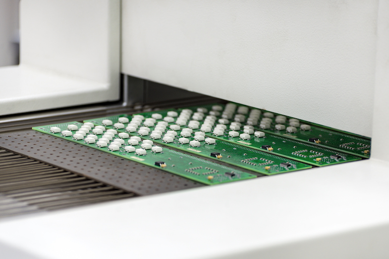
Video of Component Mount on PCB by Reflow Soldering Oven Read more about Reflow Soldering: ow.ly/4K9T50QjFXK
New! The Essential Guide to PCB Assembly Drawings: Understanding Polarities, Pin1 Marking, and Anode/Cathode Markings ow.ly/5pZo50QfVCu

Check out the new capabilities page on our website dedicated to PCB reflow soldering. 🛠️ Dive into the entire process, pitfalls+considerations, plus common issues that can arise when done without the proper processes. Check it out here: ow.ly/IjOO50PhFNR #PCBAssembly
San Francisco Circuits CEO Alex Danovich was interviewed by @Sustainmenttech & @companyweek where he discusses what led him to start SFC, why customers keep coming back after trying other PCB service providers, and more. ow.ly/y1gb50OxMU6 Profile by @sarahbrodsky

BREAKING NEWS: Over the last 20 years, global PCB production in the US has fallen from over 30% to just 4%. In response, legislators have now reintroduced the Protecting Circuit Boards and Substrates Act to help strengthen the PCB sector. Read more: ow.ly/il7t50OruZu
Frequency, transmission length, and the use of cables made from high-loss materials all contribute to insertion loss in a system's signal path. Learn how to mitigate these factors with our new PCB insertion loss resource! 🤓 ow.ly/4nz650NCx1F #insertionloss #pcbdesigning

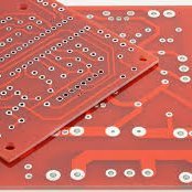
Every PCB contains at least 1 copper layer. Depending on the design requirements, the type of PCB may vary quite a bit and, as a result, the stack-up will look different too. Read more: ow.ly/OmhR50N9bgh
Many times, PCB output files and drawings are riddled with over-constrained dimensions/call-outs, improperly specified parameters, and layer counts/thicknesses based on “best guesses.” Read more: ow.ly/1pv850MVgJg


United States Trends
- 1. #BaddiesUSA 45.6K posts
- 2. Rams 26.8K posts
- 3. Cowboys 95.1K posts
- 4. Eagles 135K posts
- 5. #TROLLBOY 1,577 posts
- 6. Stafford 12.7K posts
- 7. Bucs 11.7K posts
- 8. Scotty 8,296 posts
- 9. Chip Kelly 7,149 posts
- 10. Baker 19.9K posts
- 11. Raiders 63.3K posts
- 12. #RHOP 9,783 posts
- 13. Teddy Bridgewater 1,121 posts
- 14. #ITWelcomeToDerry 12.1K posts
- 15. Stacey 28.7K posts
- 16. Todd Bowles 1,831 posts
- 17. Ahna 5,334 posts
- 18. Pickens 31K posts
- 19. Shedeur 125K posts
- 20. DOGE 151K posts
You might like
-
 Screaming Circuits
@pcbassembly -
 AcceleratedAssemblie
@acceleratedasem -
 American Std Circuit
@AmericanStdCts -
 Twisted Traces
@twistedtraces -
 Rigiflex Technology
@rigiflextech -
 ABchimie PCBA Protection
@Abchimiepcba -
 Bourns
@Bourns -
 Rush PCB UK
@rushpcbuk -
 RS DesignSpark
@RSDesignSpark -
 Global Aerospace
@GlobalAerospace
Something went wrong.
Something went wrong.