#impedancecontrol search results

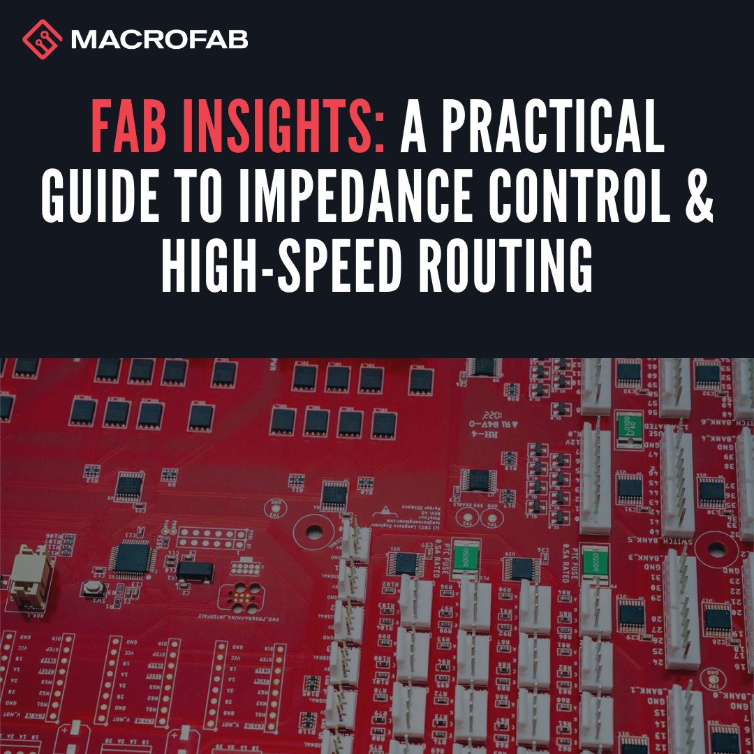
📐 High-speed signals? Impedance control isn’t optional. From USB to DDR, this guide shows when it matters and how to route for manufacturability. 👉 ow.ly/pooX50XoMR7 #PCBDesign #ImpedanceControl #ElectronicsManufacturing


Impedance control is essential in PCB assembly to maintain signal integrity & ensure optimal system performance. Precision in both design & testing is crucial to achieve the correct impedance levels. learn More: buff.ly/41tqO1D #ImpedanceControl # #CircuitDesign #PCBA

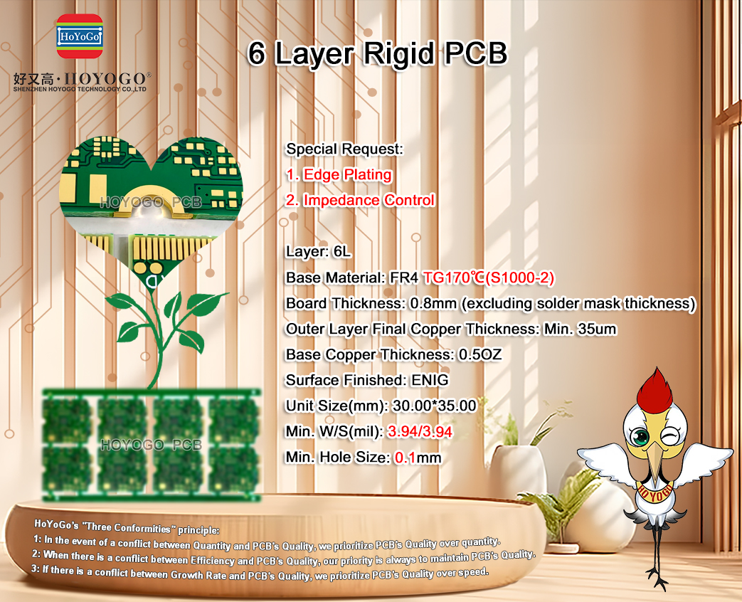
🚀 #Special Request: 📌 #EdgePlating 📌 #ImpedanceControl 🎯 #6Layer #FR4 #TG170℃(#S10002) Board Thickness: 0.8mm (excluding solder mask thickness) #OuterLayerFinalCopperThickness: Min. 35um #BaseCopperThickness: 0.5OZ Surface Finished: #ENIG Unit Size(mm): 30.00*35.00

🚀 #3StepHDIPCB ❤️🔥 🌿 The #BlindVias are located between layers L1-12, L2-L3, L3-L4, L9-L10, L10-L11, and L11-L12, as well as L9-L12. They are laser-drilled and require copper filling and capping. 🌿 #ImpedanceControl. 🌿 #BGABallPAD: 0.3mm, #BGAEllipticalPAD: 0.25mm.


#Special Request: 1. #ImpedanceControl requirements. 2. 0.25mm & 0.3mm vias: Resin plugged and electroplated filled, compliant with IPC-4761 VII. #16Layer #FR4, #IT-180A #ENIG Board Thickness: 2.58+/-0.2mm Outer Layer Final Copper Thickness: #1OZ

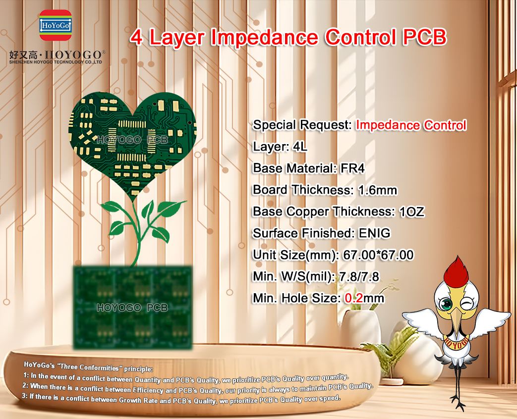
#Special Request: #ImpedanceControl #4Layer #FR4 #1OZ #ENIG Board Thickness: 1.6mm Unit Size(mm): 67.00*67.00 Min. W/S(mil): 7.8/7.8 Min. Hole Size: 0.2mm HOYOGO Website: hoyogo.com #PCBfactory #PCBmanufacturer #PCB #SMT #PCBA #PCBsupplier #AluminumPCB #HoYoGoPCB
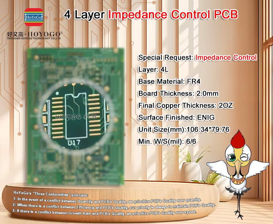
#SpecialRequest: #ImpedanceControl #4Layer #FR4 #2OZ #ENIG Board Thickness: 2.0mm Unit Size(mm):106.34*79.76 Min. W/S(mil): 6/6 HOYOGO Website: hoyogo.com Alibaba Store: hoyogo.com.cn #PCBfactory #PCBmanufacturer #PCB #SMT #PCBA #PCBsupplier #HoYoGoPCB
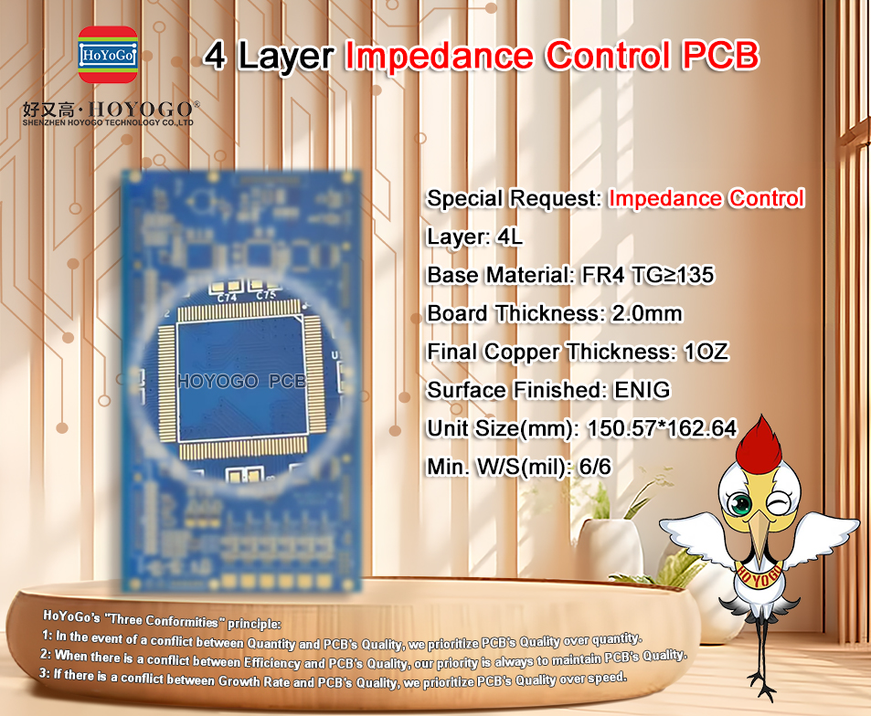
#Special Request: #ImpedanceControl #4Layer #FR4 TG≥135 #1OZ #ENIG Board Thickness: 2.0mm Unit Size(mm): 150.57*162.64 Min. W/S(mil): 6/6 HOYOGO Website: hoyogo.com Alibaba Store: hoyogo.com.cn #PCBfactory #PCBmanufacturer #PCB #FPC #PCBA #HoYoGoPCB
#Special Request: #ImpedanceControl #4Layer #FR4TG150℃ #2OZ #ENIG Board Thickness: 2.0mm Unit Size(mm): 150.57*172.62 Min. W/S(mil): 6/6 HOYOGO Website: hoyogo.com Alibaba Store: hoyogo.com.cn #PCBfactory #PCBmanufacturer #PCB #SMT #PCBA #FPC #HoYoGoPCB

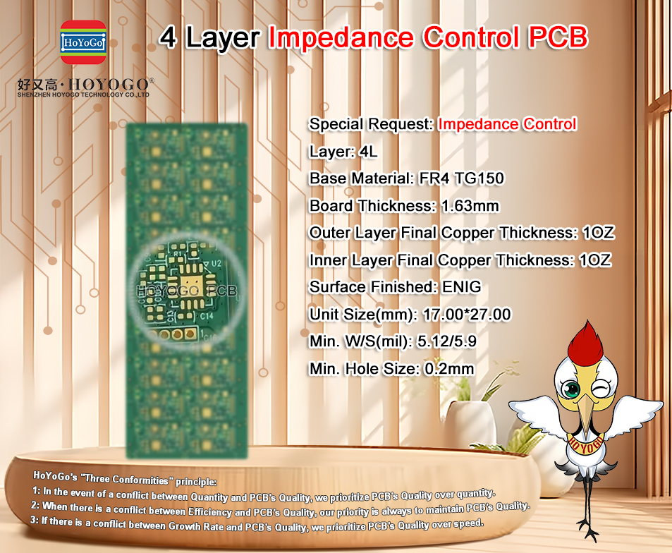
#SpecialRequest: #ImpedanceControl #4Layer #FR4TG150 #1OZ #ENIG Board Thickness: 1.63mm Unit Size(mm): 17.00*27.00 Min. W/S(mil): 5.12/5.9 Min. Hole Size: 0.2mm HOYOGO Website: hoyogo.com Alibaba Store: hoyogo.com.cn #PCBfactory #PCB #FPC #PCBA #HoYoGoPCB
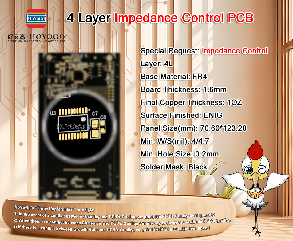
#Special Request: #ImpedanceControl #4Layer #FR4 #1OZ #ENIG #Black Board Thickness: 1.6mm Panel Size(mm): 70.60*123.20 Min. W/S(mil): 4/4.7 Min. Hole Size: 0.2mm HOYOGO Website: hoyogo.com Alibaba Store: hoyogo.com.cn #PCBfactory #PCB #PCBA #HoYoGoPCB
#Special Request: #ImpedanceControl #4Layer #FR4(#S1000-2M) #HASLLeadFree Board Thickness: 1.6mm Base Copper Thickness: 0.5OZ Unit Size(mm): 103.00*172.72 Min. W/S(mil): 6/6 HOYOGO Website: hoyogo.com hoyogo.com.cn #PCBfactory #PCBmanufacturer #HoYoGoPCB

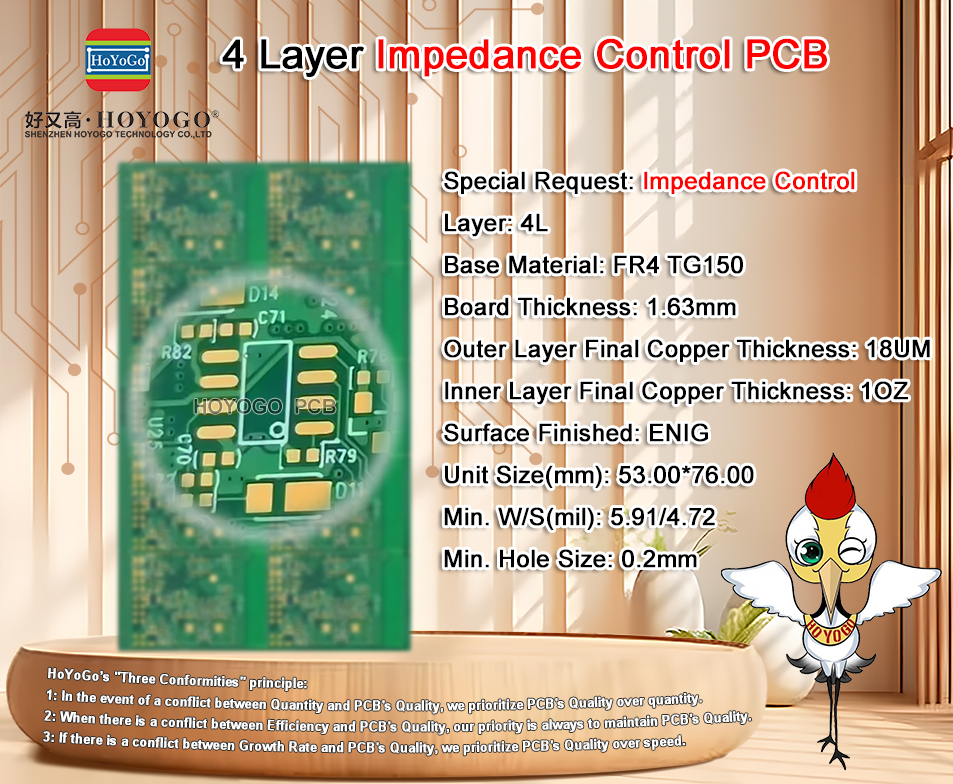
#Special Request: #ImpedanceControl #4Layer #FR4TG150 #18UM #1OZ #ENIG Board Thickness: 1.63mm Unit Size(mm): 53.00*76.00 Min. W/S(mil): 5.91/4.72 Min. Hole Size: 0.2mm HOYOGO Website: hoyogo.com Alibaba Store: hoyogo.com.cn #PCBfactory #PCB #HoYoGoPCB
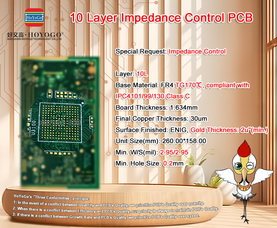
#Special Request: #ImpedanceControl #10Layer #FR4 #TG170℃, compliant with #IPC4101/99/130 Class C #30um #ENIG, #Gold Thickness: 2u"(min.) Board Thickness: 1.634mm Unit Size(mm): 260.00*158.00 Min. W/S(mil): 2.95/2.95 Min. Hole Size: 0.2mm hoyogo.com #HoYoGoPCB
Special Request: 1. There are blind and buried vias between layers L1–L3, L3–L4, and L4–L6. 2. #ImpedanceControl. #6Layer #FR4 #TG170℃(S1000-2m) #1OZ #ENIG Board Thickness: 1.54mm Unit Size(mm): 90.00*50.00 Min. W/S(mil): 3.4/5.37 Min. Hole Size: 0.15mm hoyogo.com

🔌 USB, DDR, RF? High-speed signals demand tight impedance control. Learn how to route right—with MacroFab’s design + prototyping tools. 🛠️ Start here: ow.ly/tE9j50WyPhP #PCBDesign #ImpedanceControl #HighSpeedDesign

Utilizing specific PCB sizing and impedance control for optimal performance.Designing 4-layer PCB in Altium Designer with 0.3mm hole size and 1mm diameter via options. Need help understanding via plating thickness and inductance. ##pcbmanufacturing #impedancecontrol

🚀#Special Request: 1. #EdgePlating 2. #ImpedanceControl #6Layer #FR4 #TG170℃(#S10002) #ENIG Board Thickness: 0.8mm (excluding solder mask thickness) #OuterLayerFinalCopperThickness: Min. 35um #BaseCopperThickness: 0.5OZ Min. W/S(mil): 3.94/3.94 Min. Hole Size: 0.1mm #pcb

#Article 📜 Impedance Force Control of Manipulator Based on Variable Universe Fuzzy Control by Dexin Kong and Qingjiu Huang mdpi.com/2076-0825/12/8… @kogakuin_koho @MDPIEngineering #impedancecontrol #manipulator #forcetracking #fuzzycontroller #modelreference

#Special Request: #ImpedanceControl #4Layer #FR4 #1OZ #ENIG Board Thickness: 1.6mm Unit Size(mm): 67.00*67.00 Min. W/S(mil): 7.8/7.8 Min. Hole Size: 0.2mm 💻 hoyogo.com 📬 [email protected] Welcome to send us your inquiry~ #pcb #hdi #pcba #hoyogopcb

#Special Request: #ImpedanceControl #4Layer #FR4 #1OZ #ENIG Board Thickness: 1.6mm Unit Size(mm): 67.00*67.00 Min. W/S(mil): 7.8/7.8 Min. Hole Size: 0.2mm HOYOGO Website: hoyogo.com #PCBfactory #PCBmanufacturer #PCB #SMT #PCBA #PCBsupplier #AluminumPCB #HoYoGoPCB
📐 High-speed signals? Impedance control isn’t optional. From USB to DDR, this guide shows when it matters and how to route for manufacturability. 👉 ow.ly/pooX50XoMR7 #PCBDesign #ImpedanceControl #ElectronicsManufacturing
🚀 #Special Request: 📌 #EdgePlating 📌 #ImpedanceControl 🎯 #6Layer #FR4 #TG170℃(#S10002) Board Thickness: 0.8mm (excluding solder mask thickness) #OuterLayerFinalCopperThickness: Min. 35um #BaseCopperThickness: 0.5OZ Surface Finished: #ENIG Unit Size(mm): 30.00*35.00
🔌 USB, DDR, RF? High-speed signals demand tight impedance control. Learn how to route right—with MacroFab’s design + prototyping tools. 🛠️ Start here: ow.ly/tE9j50WyPhP #PCBDesign #ImpedanceControl #HighSpeedDesign
Special Request: 1. There are blind and buried vias between layers L1–L3, L3–L4, and L4–L6. 2. #ImpedanceControl. #6Layer #FR4 #TG170℃(S1000-2m) #1OZ #ENIG Board Thickness: 1.54mm Unit Size(mm): 90.00*50.00 Min. W/S(mil): 3.4/5.37 Min. Hole Size: 0.15mm hoyogo.com
#Special Request: 1. #ImpedanceControl requirements. 2. 0.25mm & 0.3mm vias: Resin plugged and electroplated filled, compliant with IPC-4761 VII. #16Layer #FR4, #IT-180A #ENIG Board Thickness: 2.58+/-0.2mm Outer Layer Final Copper Thickness: #1OZ
#Article 📜 Impedance Force Control of Manipulator Based on Variable Universe Fuzzy Control by Dexin Kong and Qingjiu Huang mdpi.com/2076-0825/12/8… @kogakuin_koho @MDPIEngineering #impedancecontrol #manipulator #forcetracking #fuzzycontroller #modelreference

Superior noise suppression for sensitive audio electronics. No other transformer offers such a wide frequency range with such effective magnetic shielding. 👉 Learn more: hubs.ly/Q03h42m_0 #ImpedanceControl #NoiseSuppression #TechInnovation #TriadMagnetics
🚀 #3StepHDIPCB ❤️🔥 🌿 The #BlindVias are located between layers L1-12, L2-L3, L3-L4, L9-L10, L10-L11, and L11-L12, as well as L9-L12. They are laser-drilled and require copper filling and capping. 🌿 #ImpedanceControl. 🌿 #BGABallPAD: 0.3mm, #BGAEllipticalPAD: 0.25mm.
Impedance control is essential in PCB assembly to maintain signal integrity & ensure optimal system performance. Precision in both design & testing is crucial to achieve the correct impedance levels. learn More: buff.ly/41tqO1D #ImpedanceControl # #CircuitDesign #PCBA
#Article 📜 Impedance Force Control of Manipulator Based on Variable Universe Fuzzy Control by Dexin Kong and Qingjiu Huang mdpi.com/2076-0825/12/8… @kogakuin_koho @MDPIOpenAccess #impedancecontrol #manipulator #forcetracking #fuzzycontroller #modelreference
#Communication 📜 Negative-Stiffness Structure Vibration-Isolation Design and Impedance Control for a Lower Limb Exoskeleton Robot by Yaohui Sun, Jiangping Hu and Rui Huang mdpi.com/2076-0825/12/4… @UESTC1956 #impedancecontrol #negativestiffness #vibrationisolation
#Special Request: #ImpedanceControl #10Layer #FR4 #TG170℃, compliant with #IPC4101/99/130 Class C #30um #ENIG, #Gold Thickness: 2u"(min.) Board Thickness: 1.634mm Unit Size(mm): 260.00*158.00 Min. W/S(mil): 2.95/2.95 Min. Hole Size: 0.2mm hoyogo.com #HoYoGoPCB
#Article 📜 Exploring the Just Noticeable Interaction Stiffness Differences of an Impedance-Controlled Series Elastic Actuator by Rodrigo J. Velasco-Guillen, et al. mdpi.com/2076-0825/12/1… @FAU_Germany @KITKarlsruhe #justnoticeabledifference #impedancecontrol #elasticactuation

#Special Request: #ImpedanceControl #4Layer #FR4TG150℃ #2OZ #ENIG Board Thickness: 2.0mm Unit Size(mm): 150.57*172.62 Min. W/S(mil): 6/6 HOYOGO Website: hoyogo.com Alibaba Store: hoyogo.com.cn #PCBfactory #PCBmanufacturer #PCB #SMT #PCBA #FPC #HoYoGoPCB
#Special Request: #ImpedanceControl #4Layer #FR4(#S1000-2M) #HASLLeadFree Board Thickness: 1.6mm Base Copper Thickness: 0.5OZ Unit Size(mm): 103.00*172.72 Min. W/S(mil): 6/6 HOYOGO Website: hoyogo.com hoyogo.com.cn #PCBfactory #PCBmanufacturer #HoYoGoPCB
#SpecialRequest: #ImpedanceControl #4Layer #FR4TG150 #1OZ #ENIG Board Thickness: 1.63mm Unit Size(mm): 17.00*27.00 Min. W/S(mil): 5.12/5.9 Min. Hole Size: 0.2mm HOYOGO Website: hoyogo.com Alibaba Store: hoyogo.com.cn #PCBfactory #PCB #FPC #PCBA #HoYoGoPCB
📐 High-speed signals? Impedance control isn’t optional. From USB to DDR, this guide shows when it matters and how to route for manufacturability. 👉 ow.ly/pooX50XoMR7 #PCBDesign #ImpedanceControl #ElectronicsManufacturing
🔌 USB, DDR, RF? High-speed signals demand tight impedance control. Learn how to route right—with MacroFab’s design + prototyping tools. 🛠️ Start here: ow.ly/tE9j50WyPhP #PCBDesign #ImpedanceControl #HighSpeedDesign
#Article 📜 Impedance Force Control of Manipulator Based on Variable Universe Fuzzy Control by Dexin Kong and Qingjiu Huang mdpi.com/2076-0825/12/8… @kogakuin_koho @MDPIEngineering #impedancecontrol #manipulator #forcetracking #fuzzycontroller #modelreference
#Article 📜 Exploring the Just Noticeable Interaction Stiffness Differences of an Impedance-Controlled Series Elastic Actuator by Rodrigo J. Velasco-Guillen, et al. mdpi.com/2076-0825/12/1… @FAU_Germany @KITKarlsruhe #justnoticeabledifference #impedancecontrol #elasticactuation
#Communication 📜 Negative-Stiffness Structure Vibration-Isolation Design and Impedance Control for a Lower Limb Exoskeleton Robot by Yaohui Sun, Jiangping Hu and Rui Huang mdpi.com/2076-0825/12/4… @UESTC1956 #impedancecontrol #negativestiffness #vibrationisolation
Impedance control is essential in PCB assembly to maintain signal integrity & ensure optimal system performance. Precision in both design & testing is crucial to achieve the correct impedance levels. learn More: buff.ly/41tqO1D #ImpedanceControl # #CircuitDesign #PCBA
#Article ✅ Application of the Half-Order Derivative to Impedance Control of the 3-PUU #ParallelRobot 🔗doi.org/10.3390/act110… #impedancecontrol #fractionalcalculus #parallelkinematicsmachine @UniGenova @MDPIEngineering
#SpecialRequest: #ImpedanceControl #4Layer #FR4 #2OZ #ENIG Board Thickness: 2.0mm Unit Size(mm):106.34*79.76 Min. W/S(mil): 6/6 HOYOGO Website: hoyogo.com Alibaba Store: hoyogo.com.cn #PCBfactory #PCBmanufacturer #PCB #SMT #PCBA #PCBsupplier #HoYoGoPCB
#Special Request: #ImpedanceControl #4Layer #FR4 TG≥135 #1OZ #ENIG Board Thickness: 2.0mm Unit Size(mm): 150.57*162.64 Min. W/S(mil): 6/6 HOYOGO Website: hoyogo.com Alibaba Store: hoyogo.com.cn #PCBfactory #PCBmanufacturer #PCB #FPC #PCBA #HoYoGoPCB
🚀 #3StepHDIPCB ❤️🔥 🌿 The #BlindVias are located between layers L1-12, L2-L3, L3-L4, L9-L10, L10-L11, and L11-L12, as well as L9-L12. They are laser-drilled and require copper filling and capping. 🌿 #ImpedanceControl. 🌿 #BGABallPAD: 0.3mm, #BGAEllipticalPAD: 0.25mm.
🚀 #Special Request: 📌 #EdgePlating 📌 #ImpedanceControl 🎯 #6Layer #FR4 #TG170℃(#S10002) Board Thickness: 0.8mm (excluding solder mask thickness) #OuterLayerFinalCopperThickness: Min. 35um #BaseCopperThickness: 0.5OZ Surface Finished: #ENIG Unit Size(mm): 30.00*35.00
#Special Request: #ImpedanceControl #4Layer #FR4TG150℃ #2OZ #ENIG Board Thickness: 2.0mm Unit Size(mm): 150.57*172.62 Min. W/S(mil): 6/6 HOYOGO Website: hoyogo.com Alibaba Store: hoyogo.com.cn #PCBfactory #PCBmanufacturer #PCB #SMT #PCBA #FPC #HoYoGoPCB
#SpecialRequest: #ImpedanceControl #4Layer #FR4TG150 #1OZ #ENIG Board Thickness: 1.63mm Unit Size(mm): 17.00*27.00 Min. W/S(mil): 5.12/5.9 Min. Hole Size: 0.2mm HOYOGO Website: hoyogo.com Alibaba Store: hoyogo.com.cn #PCBfactory #PCB #FPC #PCBA #HoYoGoPCB
#Special Request: #ImpedanceControl #4Layer #FR4 #1OZ #ENIG #Black Board Thickness: 1.6mm Panel Size(mm): 70.60*123.20 Min. W/S(mil): 4/4.7 Min. Hole Size: 0.2mm HOYOGO Website: hoyogo.com Alibaba Store: hoyogo.com.cn #PCBfactory #PCB #PCBA #HoYoGoPCB
#Special Request: #ImpedanceControl #4Layer #FR4(#S1000-2M) #HASLLeadFree Board Thickness: 1.6mm Base Copper Thickness: 0.5OZ Unit Size(mm): 103.00*172.72 Min. W/S(mil): 6/6 HOYOGO Website: hoyogo.com hoyogo.com.cn #PCBfactory #PCBmanufacturer #HoYoGoPCB
#Special Request: #ImpedanceControl #4Layer #FR4TG150 #18UM #1OZ #ENIG Board Thickness: 1.63mm Unit Size(mm): 53.00*76.00 Min. W/S(mil): 5.91/4.72 Min. Hole Size: 0.2mm HOYOGO Website: hoyogo.com Alibaba Store: hoyogo.com.cn #PCBfactory #PCB #HoYoGoPCB
Superior noise suppression for sensitive audio electronics. No other transformer offers such a wide frequency range with such effective magnetic shielding. 👉 Learn more: hubs.ly/Q03h42m_0 #ImpedanceControl #NoiseSuppression #TechInnovation #TriadMagnetics
#Special Request: 1. #ImpedanceControl requirements. 2. 0.25mm & 0.3mm vias: Resin plugged and electroplated filled, compliant with IPC-4761 VII. #16Layer #FR4, #IT-180A #ENIG Board Thickness: 2.58+/-0.2mm Outer Layer Final Copper Thickness: #1OZ
#Special Request: #ImpedanceControl #4Layer #FR4 #1OZ #ENIG Board Thickness: 1.6mm Unit Size(mm): 67.00*67.00 Min. W/S(mil): 7.8/7.8 Min. Hole Size: 0.2mm 💻 hoyogo.com 📬 [email protected] Welcome to send us your inquiry~ #pcb #hdi #pcba #hoyogopcb
#Special Request: #ImpedanceControl #10Layer #FR4 #TG170℃, compliant with #IPC4101/99/130 Class C #30um #ENIG, #Gold Thickness: 2u"(min.) Board Thickness: 1.634mm Unit Size(mm): 260.00*158.00 Min. W/S(mil): 2.95/2.95 Min. Hole Size: 0.2mm hoyogo.com #HoYoGoPCB
Something went wrong.
Something went wrong.
United States Trends
- 1. #WWERaw 72.3K posts
- 2. Moe Odum N/A
- 3. Brock 39.2K posts
- 4. Panthers 37.3K posts
- 5. Bryce 20.8K posts
- 6. Finch 14.1K posts
- 7. Timberwolves 3,690 posts
- 8. 49ers 41.2K posts
- 9. Gonzaga 3,941 posts
- 10. Canales 13.2K posts
- 11. Keegan Murray 1,351 posts
- 12. Penta 10.5K posts
- 13. Niners 5,793 posts
- 14. #FTTB 5,769 posts
- 15. Mac Jones 4,928 posts
- 16. Amen Thompson 2,109 posts
- 17. Malik Monk N/A
- 18. Gunther 15.2K posts
- 19. Jauan Jennings 2,784 posts
- 20. Zags N/A