#pcblayers search results

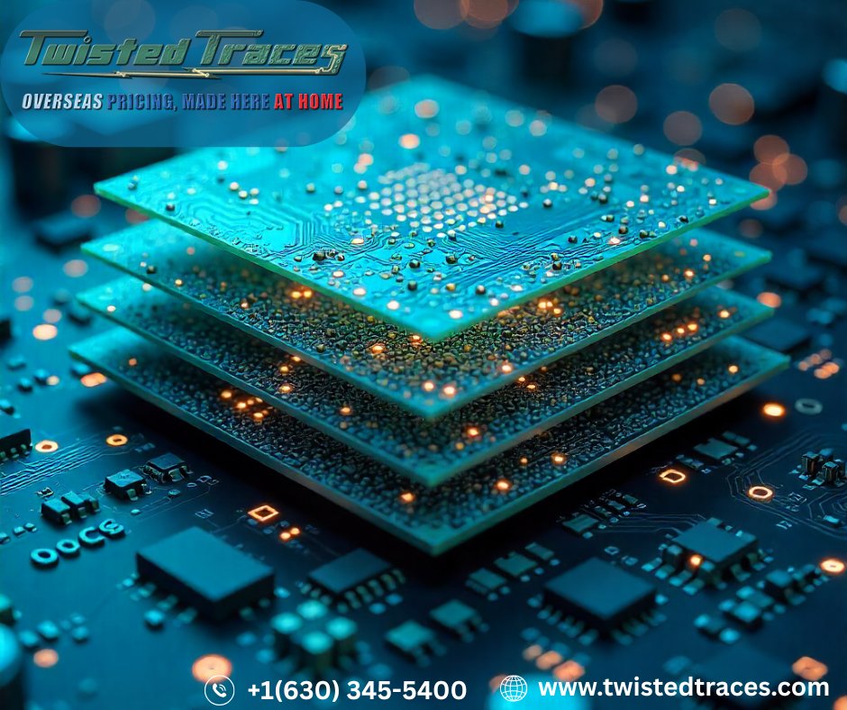
PCB Layers Capabilities Twisted Traces manufactures PCBs from 1 to 20 layers in FR-4, FR-406, and 370HR, and 1–2 layer boards in Rogers, Aluminum/Copper, and Teflon. Copper thickness can be customized to your exact requirements. Read More: bit.ly/46LBrPU #PCB #PCBLayers


PCB & Circuit Design & Drafting Training – Learn Digital/Analogue Circuit Design, #PCBRouting Diagram, #PCBLayers & Grounding. Call us 9873684099 or email us [email protected] or visit buff.ly/2AqFrUx #PcbDesign #PcbTrainingInstitute


PCB layers explained in the most basic terms consist of interspersed conductive and insulative layers, but that only scratches the surface. #pcba #pcblayers vse.com/blog/2022/09/2…

Are Gerber files of inner layers interchangeable? electronics.stackexchange.com/q/353713?atw=1 #pcblayers
Mechanical construction of PCB. What is between the layers? electronics.stackexchange.com/q/585198?atw=1 #pcblayers

An Overview of Layer Stack Management in PCB Design circuitdigest.com/article/an-ove… #pcb #pcbdesign #pcblayers #multilayerpcb

Understanding PCB layers is key to quality design. From substrate to silkscreen, each part ensures functionality. Discover more with ABL Circuits: eu1.hubs.ly/H0dZ-Dl0 #PCBDesign #PCBLayers #Electronics

Understanding the standard PCB layer stack-up is crucial for successful PCB design. With the right layer configuration, for optimize your board's performance and ensure reliable operation:bit.ly/3KasHrl #PCBdesign #PCBstackup #PCBlayers #circuitboard #PCBconfiguration
PCB Layers Capabilities Twisted Traces manufactures PCBs from 1 to 20 layers in FR-4, FR-406, and 370HR, and 1–2 layer boards in Rogers, Aluminum/Copper, and Teflon. Copper thickness can be customized to your exact requirements. Read More: bit.ly/46LBrPU #PCB #PCBLayers
Understanding PCB layers is key to quality design. From substrate to silkscreen, each part ensures functionality. Discover more with ABL Circuits: eu1.hubs.ly/H0dZ-Dl0 #PCBDesign #PCBLayers #Electronics
Understanding the standard PCB layer stack-up is crucial for successful PCB design. With the right layer configuration, for optimize your board's performance and ensure reliable operation:bit.ly/3KasHrl #PCBdesign #PCBstackup #PCBlayers #circuitboard #PCBconfiguration
PCB layers explained in the most basic terms consist of interspersed conductive and insulative layers, but that only scratches the surface. #pcba #pcblayers vse.com/blog/2022/09/2…
Mechanical construction of PCB. What is between the layers? electronics.stackexchange.com/q/585198?atw=1 #pcblayers
An Overview of Layer Stack Management in PCB Design circuitdigest.com/article/an-ove… #pcb #pcbdesign #pcblayers #multilayerpcb
Are Gerber files of inner layers interchangeable? electronics.stackexchange.com/q/353713?atw=1 #pcblayers
PCB & Circuit Design & Drafting Training – Learn Digital/Analogue Circuit Design, #PCBRouting Diagram, #PCBLayers & Grounding. Call us 9873684099 or email us [email protected] or visit buff.ly/2AqFrUx #PcbDesign #PcbTrainingInstitute
PCB Layers Capabilities Twisted Traces manufactures PCBs from 1 to 20 layers in FR-4, FR-406, and 370HR, and 1–2 layer boards in Rogers, Aluminum/Copper, and Teflon. Copper thickness can be customized to your exact requirements. Read More: bit.ly/46LBrPU #PCB #PCBLayers
PCB layers explained in the most basic terms consist of interspersed conductive and insulative layers, but that only scratches the surface. #pcba #pcblayers vse.com/blog/2022/09/2…
PCB & Circuit Design & Drafting Training – Learn Digital/Analogue Circuit Design, #PCBRouting Diagram, #PCBLayers & Grounding. Call us 9873684099 or email us [email protected] or visit buff.ly/2AqFrUx #PcbDesign #PcbTrainingInstitute
Understanding PCB layers is key to quality design. From substrate to silkscreen, each part ensures functionality. Discover more with ABL Circuits: eu1.hubs.ly/H0dZ-Dl0 #PCBDesign #PCBLayers #Electronics
Something went wrong.
Something went wrong.
United States Trends
- 1. Knicks 12.4K posts
- 2. Landry Shamet 1,189 posts
- 3. #AEWDynamite 20.7K posts
- 4. Philon 1,732 posts
- 5. Brandon Williams N/A
- 6. #Survivor49 3,690 posts
- 7. #CMAawards 5,280 posts
- 8. #AEWCollision 8,306 posts
- 9. Vucevic 4,913 posts
- 10. Vooch 1,022 posts
- 11. Blazers 3,983 posts
- 12. Derik Queen 3,410 posts
- 13. #mnwild N/A
- 14. Simon Walker N/A
- 15. Wallstedt N/A
- 16. Dubon 3,655 posts
- 17. Donovan Mitchell 3,910 posts
- 18. Bristow 1,087 posts
- 19. Jackson Blake N/A
- 20. Coby White N/A