#pcbtips hasil pencarian

GHz isn’t everything ⚙️ A well-designed board lives or dies on: 🔹 signal integrity 🔹 power stability 🔹 EMI discipline Clean layout is performance. Ask any hardware dev after 2 a.m 😤 #EmbeddedDesign #PCBtips


A quick look at common and unexpected PCB assembly challenges, with simple tips to help you avoid errors and improve reliability. #pcbassembly #electronicsmanufacturing #pcbtips #hardwareengineering #TechGuide Read blog for more information- medium.com/@pcbpower01/ov…
medium.com
Overcoming Common (& Less Common) PCB Assembly Challenges
PCB assembly is vital to converting a blank board into an electronic system. Even minor errors during the assembly process can result in…

👀 Ever heard of C-shaped pads in PCB? 🎯 Order your custom PCB : allpcb.com/?code=S25 #PCBtips #SMTdesign #ElectronicsDesign #ALLPCB

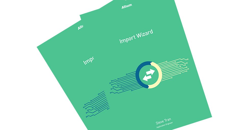
What if you could quickly import a PCB design from one platform to another without ANY errors? ow.ly/s3To304JXxe #PCBtips

IRevive your gadgets instead of tossing them! 🛠️ Learn practical PCB repair tips, prevent damage, and extend your electronics' life—saving money and reducing e-waste. #PCBTips #ElectronicsRepair #DIYElectronics medium.com/p/save-your-el…

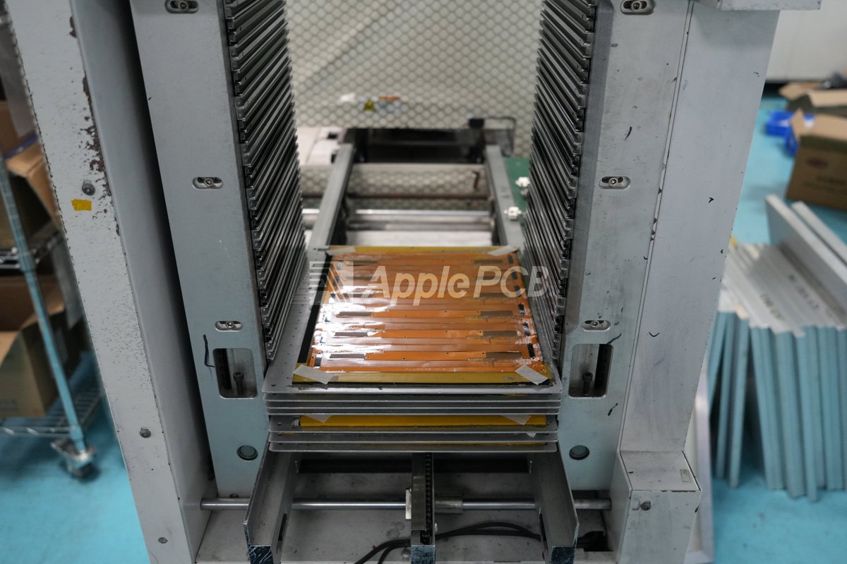
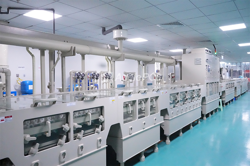
How to solve the problem of wrinkled ultra-thin copper foil lamination? 📍 Elimination of adhesive barrier points: The 1cm adhesive barrier area around the rivet formed a flow groove, allowing the PP adhesive to flow naturally and stretch the copper foil.#ApplePCB #PCBTips

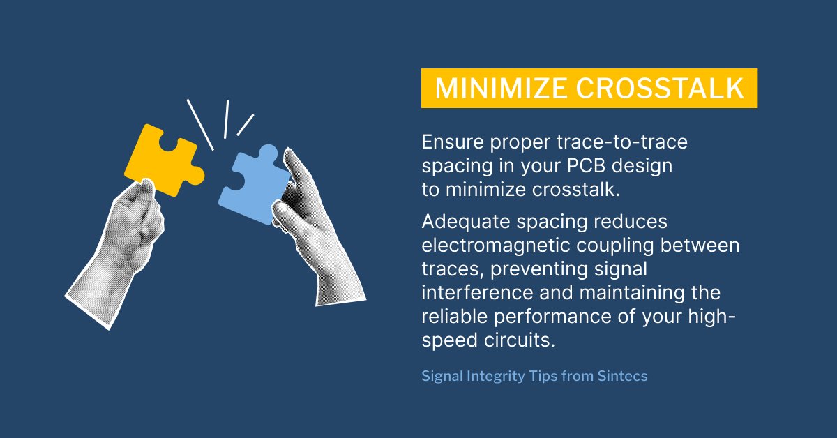
Minimize crosstalk in your PCB designs by ensuring proper trace-to-trace spacing. Fair spacing helps reduce electromagnetic coupling, ensuring reliable performance and signal integrity in high-speed circuits. #PCBTips #SignalIntegrity #PCBDesign #ElectronicsEngineering #Sintecs


Read this article to learn how to design printed circuit boards using vias. ow.ly/nPSR30eTQUw #PCBDesign #PCBTips

Why Is Your PCB Warping? 🤔 Let's Explore the Causes from a PCB Manufacturer's Perspective. 1️⃣ No Baking or Insufficient Baking Time 2️⃣ Excessively Deep V-CUT 3️⃣ Low TG Material 4️⃣ Thin Boards (<1.0mm) More Info: applepcb.com #ApplePCB #PCBManufacturing #PCBTips

Cada capa de tu diseño PCB cuenta, recuerda considerar cuidadosamente su señal y su propósito a tierra. Consejo extra: Menos Vueltas, Más Seguridad. Evita interferencias electromagnéticas. 🤓💡 #TecnoConCiencia #PCBTips

What is a Burn-In Printed Circuit Board (PCB)? A Burn-in PCB is a printed-circuit board that undergoes a burn-in testing process. Continue to read: ow.ly/WW1050VNoTl #BurnInPCB #PCBTips #ElectronicsTesting #PCBManufacturing #FR4Materials #PCBDirectory #TechArticle


Avoiding Typical Errors in PCB Design‼️👇 #AvoidPCBFails #PCBTips #ElectronicsTips #CircuitDesign

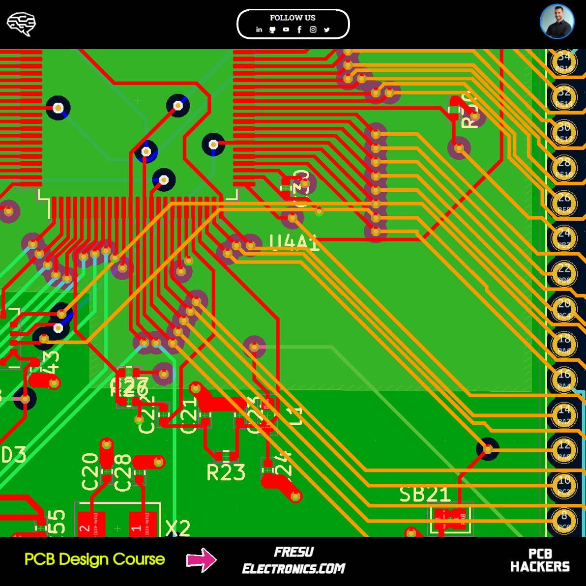
𝗘𝗹𝗲𝗰𝘁𝗿𝗼𝗻𝗶𝗰 𝗰𝗶𝗿𝗰𝘂𝗶𝘁 𝗱𝗲𝘀𝗶𝗴𝗻𝗲𝗿𝘀, don't make this PCB design mistake when trying to route your board. Yeah, I also thought it was so simple. When I first started designing Printed Circuit Boards, I thought that converting my electrical schematics'…

"What’s your go-to hardware development hack? I’ll start: Never route the PCB first. Share the component placement and STL with the mechanical team, freeze the placement, then begin routing. #HardwareDesign #PCBtips #ElectronicsDev"

#PCBtips from @tpelli7 & @madeline319: don't go to jail, don't passout on the beach & burn, don't get pregnant/STD, meet lots of cute boys &

Get the very best of your PCB prototyping experience. Check out the article for the essential tips. #PCBtips #PCB bit.ly/2tGNg7T

#PCBtips Buy burnettes, put it through a brita filter, comes out tasting like smirnoff. Think I'm kidding? Try it.
#PCBTips Book Early we got a major deal with @HolidayInnPCB #shoutout
A quick look at common and unexpected PCB assembly challenges, with simple tips to help you avoid errors and improve reliability. #pcbassembly #electronicsmanufacturing #pcbtips #hardwareengineering #TechGuide Read blog for more information- medium.com/@pcbpower01/ov…
medium.com
Overcoming Common (& Less Common) PCB Assembly Challenges
PCB assembly is vital to converting a blank board into an electronic system. Even minor errors during the assembly process can result in…
GHz isn’t everything ⚙️ A well-designed board lives or dies on: 🔹 signal integrity 🔹 power stability 🔹 EMI discipline Clean layout is performance. Ask any hardware dev after 2 a.m 😤 #EmbeddedDesign #PCBtips
Why Is Your PCB Warping? 🤔 Let's Explore the Causes from a PCB Manufacturer's Perspective. 1️⃣ No Baking or Insufficient Baking Time 2️⃣ Excessively Deep V-CUT 3️⃣ Low TG Material 4️⃣ Thin Boards (<1.0mm) More Info: applepcb.com #ApplePCB #PCBManufacturing #PCBTips
👀 Ever heard of C-shaped pads in PCB? 🎯 Order your custom PCB : allpcb.com/?code=S25 #PCBtips #SMTdesign #ElectronicsDesign #ALLPCB
"What’s your go-to hardware development hack? I’ll start: Never route the PCB first. Share the component placement and STL with the mechanical team, freeze the placement, then begin routing. #HardwareDesign #PCBtips #ElectronicsDev"
What is a Burn-In Printed Circuit Board (PCB)? A Burn-in PCB is a printed-circuit board that undergoes a burn-in testing process. Continue to read: ow.ly/WW1050VNoTl #BurnInPCB #PCBTips #ElectronicsTesting #PCBManufacturing #FR4Materials #PCBDirectory #TechArticle
How to solve the problem of wrinkled ultra-thin copper foil lamination? 📍 Elimination of adhesive barrier points: The 1cm adhesive barrier area around the rivet formed a flow groove, allowing the PP adhesive to flow naturally and stretch the copper foil.#ApplePCB #PCBTips
Minimize crosstalk in your PCB designs by ensuring proper trace-to-trace spacing. Fair spacing helps reduce electromagnetic coupling, ensuring reliable performance and signal integrity in high-speed circuits. #PCBTips #SignalIntegrity #PCBDesign #ElectronicsEngineering #Sintecs
Cada capa de tu diseño PCB cuenta, recuerda considerar cuidadosamente su señal y su propósito a tierra. Consejo extra: Menos Vueltas, Más Seguridad. Evita interferencias electromagnéticas. 🤓💡 #TecnoConCiencia #PCBTips
Avoiding Typical Errors in PCB Design‼️👇 #AvoidPCBFails #PCBTips #ElectronicsTips #CircuitDesign
𝗘𝗹𝗲𝗰𝘁𝗿𝗼𝗻𝗶𝗰 𝗰𝗶𝗿𝗰𝘂𝗶𝘁 𝗱𝗲𝘀𝗶𝗴𝗻𝗲𝗿𝘀, don't make this PCB design mistake when trying to route your board. Yeah, I also thought it was so simple. When I first started designing Printed Circuit Boards, I thought that converting my electrical schematics'…
Read this article to learn how to design printed circuit boards using vias. ow.ly/nPSR30eTQUw #PCBDesign #PCBTips
Get the very best of your PCB prototyping experience. Check out the article for the essential tips. #PCBtips #PCB bit.ly/2tGNg7T

GHz isn’t everything ⚙️ A well-designed board lives or dies on: 🔹 signal integrity 🔹 power stability 🔹 EMI discipline Clean layout is performance. Ask any hardware dev after 2 a.m 😤 #EmbeddedDesign #PCBtips
What if you could quickly import a PCB design from one platform to another without ANY errors? ow.ly/s3To304JXxe #PCBtips
Minimize crosstalk in your PCB designs by ensuring proper trace-to-trace spacing. Fair spacing helps reduce electromagnetic coupling, ensuring reliable performance and signal integrity in high-speed circuits. #PCBTips #SignalIntegrity #PCBDesign #ElectronicsEngineering #Sintecs
How to solve the problem of wrinkled ultra-thin copper foil lamination? 📍 Elimination of adhesive barrier points: The 1cm adhesive barrier area around the rivet formed a flow groove, allowing the PP adhesive to flow naturally and stretch the copper foil.#ApplePCB #PCBTips
Read this article to learn how to design printed circuit boards using vias. ow.ly/nPSR30eTQUw #PCBDesign #PCBTips
What is a Burn-In Printed Circuit Board (PCB)? A Burn-in PCB is a printed-circuit board that undergoes a burn-in testing process. Continue to read: ow.ly/WW1050VNoTl #BurnInPCB #PCBTips #ElectronicsTesting #PCBManufacturing #FR4Materials #PCBDirectory #TechArticle
Why Is Your PCB Warping? 🤔 Let's Explore the Causes from a PCB Manufacturer's Perspective. 1️⃣ No Baking or Insufficient Baking Time 2️⃣ Excessively Deep V-CUT 3️⃣ Low TG Material 4️⃣ Thin Boards (<1.0mm) More Info: applepcb.com #ApplePCB #PCBManufacturing #PCBTips
Something went wrong.
Something went wrong.
United States Trends
- 1. Davis Mills 3,888 posts
- 2. Texans 28.5K posts
- 3. Josh Allen 12.4K posts
- 4. Ray Davis 1,800 posts
- 5. #MissUniverse 104K posts
- 6. #TNFonPrime 1,752 posts
- 7. Taron Johnson N/A
- 8. Christian Kirk 3,019 posts
- 9. James Cook 4,665 posts
- 10. Nico Collins 1,546 posts
- 11. Cole Bishop N/A
- 12. Sedition 245K posts
- 13. Will Anderson 3,000 posts
- 14. Shakir 3,594 posts
- 15. Jayden Higgins N/A
- 16. Cam Lewis N/A
- 17. #htownmade 1,664 posts
- 18. Maxey 2,981 posts
- 19. Woody Marks 2,385 posts
- 20. #BUFvsHOU 1,922 posts