#semivision 검색 결과


Feeling proud today 💡 Seeing our #SemiVision graphics being cited by securities firms around the world and written into industry research reports reminds me that our influence is slowly but steadily growing. It’s a small but powerful validation of the work we do — from deep…

✨ Today at SEMICON Taiwan, I spent time walking through Hall 1 at Nangang Exhibition Center, both the 1st and 4th floors. When I handed out my #SemiVision business card, I was pleasantly surprised to find that many people already follow me. That moment truly made me feel happy…


🍱 Disco used the analogy of a bento box to explain the importance of panel-level packaging. A very creative and fun way to illustrate a complex semiconductor concept! Photo by #SemiVision #Semicon #AdvancedPackaging #PLP #Disco

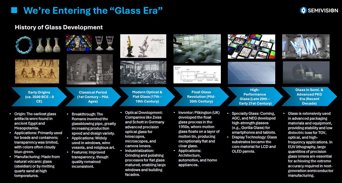
🥃#SemiVision: Today I had the honor of giving a talk at the #HICHIP Alliance, with the topic:“From Sand to Silicon — and Now to #Glass: The Evolution of Chip Packaging.” This slide is something I spent a lot of time putting together. While preparing it, I also gained a much…
🔵Attended the #TPCA Technology Forum and saw Professor hao-chung kuo using our #SemiVision image to introduce EIC/PIC integration. Looking forward to creating more silicon photonics visuals to share insights on the industry ecosystem with everyone. Welcome to subscribe our…

🟥 Henkel - Comparison of Interposer Options #SemiVision : The matrix highlights that no single interposer technology is perfect—each brings trade-offs. ▪️Silicon interposers excel in bandwidth, but face cost and size constraints. ▪️RDL panels offer cost advantages, though…

🔥#SemiVision : Recently, there have been numerous rumors about #NVIDIA ’s next-generation chip Rubin, including a reported increase in TDP (Total Design Power) from 1,800W to 2,300W. To cope with the 27.7% rise in power consumption, the cooling solution is said to shift from a…

🟩#SemiVision : The packaging evolution trend in response to the increasing demands of #AI workloads, which require significantly larger package sizes and more complex substrate architectures. As chiplet-based and MCM (multi-chip module) designs continue to advance, #substrate…

Invited to attend the 5th Advanced Materials Manufacturing Technology Forum 2025 at National Chin-Yi University of Technology. #semivision #Semiconductor

🍰#SemiVision: To meet the growing demand for HPC and AI accelerators, researchers are advancing die-to-wafer (D2W) hybrid Cu bonding and wafer reconstruction processes for ultra-dense 3D ICs. Key breakthroughs include: ◾ 2 μm bond pad pitch for D2W HCB ◾ Island die grinding…

Thank you all for your incredible support! 🎉 #SEMIVISION is now ranked #36 on the #Substack Technology leaderboard. We’ll keep pushing forward—this is just the beginning. substack.com/@semivision?r=…
#SemiVision is a semiconductor industry research institution dedicated to transforming detailed analysis into clear, actionable vision. Through comprehensive insights across design, fabrication, packaging, testing, and supply chains, it empowers industry stakeholders with…

📚 From Packaging to Platform: #ECTC and #IEDM Lead the Era of System-Level Integration #SemiVision: As the global electronics industry moves into a new wave driven by #AI and high-performance computing (#HPC), advanced packaging technologies are quietly becoming the…

#SemiVision: From Packaging to Platform: #ECTC and #IEDM Lead the Era of System-Level Integration open.substack.com/pub/tspasemico…

📌 #SemiVision: #Advantest Taiwan Sales Surge, Driven by #AI Demand In the latest quarterly results, Advantest's sales in Taiwan jumped from JPY 41.5B in FY24 Q1 to JPY 162.1B in FY25 Q1 — a 4X increase in just one year. This growth highlights Taiwan's central role in the global…

🍱 Disco used the analogy of a bento box to explain the importance of panel-level packaging. A very creative and fun way to illustrate a complex semiconductor concept! Photo by #SemiVision #Semicon #AdvancedPackaging #PLP #Disco
🔥#SemiVision : Recently, there have been numerous rumors about #NVIDIA ’s next-generation chip Rubin, including a reported increase in TDP (Total Design Power) from 1,800W to 2,300W. To cope with the 27.7% rise in power consumption, the cooling solution is said to shift from a…
✨ Today at SEMICON Taiwan, I spent time walking through Hall 1 at Nangang Exhibition Center, both the 1st and 4th floors. When I handed out my #SemiVision business card, I was pleasantly surprised to find that many people already follow me. That moment truly made me feel happy…
🟥 Henkel - Comparison of Interposer Options #SemiVision : The matrix highlights that no single interposer technology is perfect—each brings trade-offs. ▪️Silicon interposers excel in bandwidth, but face cost and size constraints. ▪️RDL panels offer cost advantages, though…
Feeling proud today 💡 Seeing our #SemiVision graphics being cited by securities firms around the world and written into industry research reports reminds me that our influence is slowly but steadily growing. It’s a small but powerful validation of the work we do — from deep…
🥃#SemiVision: Today I had the honor of giving a talk at the #HICHIP Alliance, with the topic:“From Sand to Silicon — and Now to #Glass: The Evolution of Chip Packaging.” This slide is something I spent a lot of time putting together. While preparing it, I also gained a much…
Invited to attend the 5th Advanced Materials Manufacturing Technology Forum 2025 at National Chin-Yi University of Technology. #semivision #Semiconductor
📌 #SemiVision: #Advantest Taiwan Sales Surge, Driven by #AI Demand In the latest quarterly results, Advantest's sales in Taiwan jumped from JPY 41.5B in FY24 Q1 to JPY 162.1B in FY25 Q1 — a 4X increase in just one year. This growth highlights Taiwan's central role in the global…
#SemiVision is a semiconductor industry research institution dedicated to transforming detailed analysis into clear, actionable vision. Through comprehensive insights across design, fabrication, packaging, testing, and supply chains, it empowers industry stakeholders with…
According to #SemiVision Research, PIC fabrication requires around 30+ mask layers, with key components including waveguides, GePD (Germanium Photodetectors), and modulators. Modulators adjust optical properties, and their fabrication involves ion implantation, requiring specific…
🍰#SemiVision: To meet the growing demand for HPC and AI accelerators, researchers are advancing die-to-wafer (D2W) hybrid Cu bonding and wafer reconstruction processes for ultra-dense 3D ICs. Key breakthroughs include: ◾ 2 μm bond pad pitch for D2W HCB ◾ Island die grinding…
🔵Attended the #TPCA Technology Forum and saw Professor hao-chung kuo using our #SemiVision image to introduce EIC/PIC integration. Looking forward to creating more silicon photonics visuals to share insights on the industry ecosystem with everyone. Welcome to subscribe our…
Thank you all for your incredible support! 🎉 #SEMIVISION is now ranked #36 on the #Substack Technology leaderboard. We’ll keep pushing forward—this is just the beginning. substack.com/@semivision?r=…
🟩#SemiVision : The packaging evolution trend in response to the increasing demands of #AI workloads, which require significantly larger package sizes and more complex substrate architectures. As chiplet-based and MCM (multi-chip module) designs continue to advance, #substrate…
🟧#SemiVision : At the 2025 #IEEE #VLSI Symposium, a pivotal panel presentation led by MediaTek clearly outlined the company’s comprehensive strategy across four key axes: #AI #ASIC design, intelligent edge, automotive platforms, and #CPO (co-packaged optics) interconnects. This…

📚 From Packaging to Platform: #ECTC and #IEDM Lead the Era of System-Level Integration #SemiVision: As the global electronics industry moves into a new wave driven by #AI and high-performance computing (#HPC), advanced packaging technologies are quietly becoming the…
#SemiVision: From Packaging to Platform: #ECTC and #IEDM Lead the Era of System-Level Integration open.substack.com/pub/tspasemico…


🛑 Want to give old photos a new life? 🛑 ⚜️ Use Google Gemini Ai ⚜️ Note: This is not a free AI filter. It’s a professional restoration service where each photo is enhanced. DM me for packages. Prompt , Please edit my old photo into 1080 x 1920 pixels, with an aesthetic…


🍱 Disco used the analogy of a bento box to explain the importance of panel-level packaging. A very creative and fun way to illustrate a complex semiconductor concept! Photo by #SemiVision #Semicon #AdvancedPackaging #PLP #Disco

Since we got a new Artist kit I want to share the "Set Filters on Paintings by Reference mod". A must have mod for me! I always use it for legacy sims. You can do sepia, black and white, and more. I don't like the grainy look because you can barely make out details. Link below!


I love the way this filter gives photos a painting aesthetic. She's so beautiful!


🔵Attended the #TPCA Technology Forum and saw Professor hao-chung kuo using our #SemiVision image to introduce EIC/PIC integration. Looking forward to creating more silicon photonics visuals to share insights on the industry ecosystem with everyone. Welcome to subscribe our…
🌈#SemiVision : As #AI, cloud computing, and data center workloads continue to surge, traditional copper-based SerDes links are reaching their limits in terms of bandwidth, power efficiency, and short-reach interconnect scalability. Co-Packaged Optics (#CPO) has emerged as the…

Something went wrong.
Something went wrong.
United States Trends
- 1. Good Sunday 54K posts
- 2. #sundayvibes 4,763 posts
- 3. #AskBetr N/A
- 4. Muhammad Qasim 8,841 posts
- 5. Discussing Web3 N/A
- 6. Wordle 1,576 X N/A
- 7. #HealingFromMozambique 20.5K posts
- 8. Miary Zo 1,234 posts
- 9. Trump's FBI 12.2K posts
- 10. KenPom N/A
- 11. Biden FBI 18.9K posts
- 12. Blessed Sunday 17.7K posts
- 13. Coco 48.7K posts
- 14. #ChicagoMarathon N/A
- 15. Mason Taylor N/A
- 16. The CDC 33K posts
- 17. Lord's Day 1,688 posts
- 18. Gilligan 7,205 posts
- 19. Macrohard 9,799 posts
- 20. Go Broncos 1,327 posts