#twolayerpcb search results

#twolayerpcb #4gmodule with #quectelwireless #EG91 #wirelessmodule. It can be done, and it has been done for my friend Raper, who will soon use these modules in an #automotiveelectronics application. While I do not have the final… 📸 instagram.com/p/CWFThavNcdG/

#componentplacement is extremely important. Always look at your #ratsnest when doing the layout. Here, the difference between a #twolayerpcb and a #fourlayerpcb was correct positioning of the #SMDleds. #target3001 currently is a bit buggy… 📸 instagram.com/p/CCIWpVYD0Fj/

#QuecTel #ltemodule done, on a #twolayerpcb and with #smaconnector at customer request. This was quite a job, as we started out with #telit, moved on to #Ublox and finally selected the #bg96. In the end, this was the best possible decision - the… 📸 instagram.com/p/CHFQ3FZDIup/

#idioticmistake. Set up a #via, and then continue the track on the wrong side of the #twolayerpcb. Blame it on age, senility or overworkedness? Layout system is #target3001, and I do wonder why it did not catch this - normally, it moans even if you… 📸 instagram.com/p/CB05bJZDWnZ/

Preparation is half the #SMD #prototyperun. When working on a #twolayerpcb, I personally like to use a #highlightmarker to break up the #electroniccomponents into two parts. Then, a #buildingtrashcan is assembled for each run...and yes, I know that… 📸 instagram.com/p/Ce_BE2hL9cT/


💡 Why Trust Us? ✔️ Decades of experience ✔️ Advanced manufacturing techniques ✔️ Reliable quality assurance 📞 Get Your Custom Two-Layer PCB Designed Today! #TwoLayerPCB #PCBProblems #PCBDesignSolutions #Innovation #ElectronicsManufacturing

The evolution of PCB design software has revolutionized the way engineers create and optimize circuit boards. Modern PCB design software includes several key advancements: #TwoLayerPCB #PCBProblems #PCBDesignSolutions #Innovation #ElectronicsManufacturing


Power Electronics News explores MPS’s MPQ4323-AEC1 with an overview of the schematic and layout designs for a two-layer PCB. #AspenCore #TwoLayerPCB #PCBDesign powerelectronicsnews.com/pen-november-e…
High-Layer Count (HLC) PCBoard #PrintedCircuitBoard #twolayerPCB #highlayercountPCBorprintedcircuitboardassembly Read more: bit.ly/3MEPzPm Location: 115 East Centre St. Nutley, NJ, 07110 Call us: (973) 284-1600 Email us: [email protected]
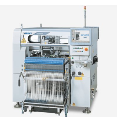
Ideal for advanced projects requiring multiple layers, our stencils ensure perfect alignment and accurate solder paste application on each layer. Visit Us- bit.ly/4cJDJjm #PCBSTencils #TwoLayerPCB #CircuitDesign #ElectronicsManufacturing #PCBAssembly #EngineeringTools

At Pcbcircuit, we make prototype PCB manufacturing the easiest way for your business! Visit Now: bit.ly/3Cf7uej #TwoLayerPCB #PCBProblems #PCBDesignSolutions #Innovation #ElectronicsManufacturing

The evolution of PCB design software has revolutionized the way engineers create and optimize circuit boards. Modern PCB design software includes several key advancements: #TwoLayerPCB #PCBProblems #PCBDesignSolutions #Innovation #ElectronicsManufacturing
At Pcbcircuit, we make prototype PCB manufacturing the easiest way for your business! Visit Now: bit.ly/3Cf7uej #TwoLayerPCB #PCBProblems #PCBDesignSolutions #Innovation #ElectronicsManufacturing
💡 Why Trust Us? ✔️ Decades of experience ✔️ Advanced manufacturing techniques ✔️ Reliable quality assurance 📞 Get Your Custom Two-Layer PCB Designed Today! #TwoLayerPCB #PCBProblems #PCBDesignSolutions #Innovation #ElectronicsManufacturing
Ideal for advanced projects requiring multiple layers, our stencils ensure perfect alignment and accurate solder paste application on each layer. Visit Us- bit.ly/4cJDJjm #PCBSTencils #TwoLayerPCB #CircuitDesign #ElectronicsManufacturing #PCBAssembly #EngineeringTools
Power Electronics News explores MPS’s MPQ4323-AEC1 with an overview of the schematic and layout designs for a two-layer PCB. #AspenCore #TwoLayerPCB #PCBDesign powerelectronicsnews.com/pen-november-e…
High-Layer Count (HLC) PCBoard #PrintedCircuitBoard #twolayerPCB #highlayercountPCBorprintedcircuitboardassembly Read more: bit.ly/3MEPzPm Location: 115 East Centre St. Nutley, NJ, 07110 Call us: (973) 284-1600 Email us: [email protected]
Preparation is half the #SMD #prototyperun. When working on a #twolayerpcb, I personally like to use a #highlightmarker to break up the #electroniccomponents into two parts. Then, a #buildingtrashcan is assembled for each run...and yes, I know that… 📸 instagram.com/p/Ce_BE2hL9cT/
#twolayerpcb #4gmodule with #quectelwireless #EG91 #wirelessmodule. It can be done, and it has been done for my friend Raper, who will soon use these modules in an #automotiveelectronics application. While I do not have the final… 📸 instagram.com/p/CWFThavNcdG/
#QuecTel #ltemodule done, on a #twolayerpcb and with #smaconnector at customer request. This was quite a job, as we started out with #telit, moved on to #Ublox and finally selected the #bg96. In the end, this was the best possible decision - the… 📸 instagram.com/p/CHFQ3FZDIup/
#componentplacement is extremely important. Always look at your #ratsnest when doing the layout. Here, the difference between a #twolayerpcb and a #fourlayerpcb was correct positioning of the #SMDleds. #target3001 currently is a bit buggy… 📸 instagram.com/p/CCIWpVYD0Fj/
#idioticmistake. Set up a #via, and then continue the track on the wrong side of the #twolayerpcb. Blame it on age, senility or overworkedness? Layout system is #target3001, and I do wonder why it did not catch this - normally, it moans even if you… 📸 instagram.com/p/CB05bJZDWnZ/
#twolayerpcb #4gmodule with #quectelwireless #EG91 #wirelessmodule. It can be done, and it has been done for my friend Raper, who will soon use these modules in an #automotiveelectronics application. While I do not have the final… 📸 instagram.com/p/CWFThavNcdG/
#componentplacement is extremely important. Always look at your #ratsnest when doing the layout. Here, the difference between a #twolayerpcb and a #fourlayerpcb was correct positioning of the #SMDleds. #target3001 currently is a bit buggy… 📸 instagram.com/p/CCIWpVYD0Fj/
#QuecTel #ltemodule done, on a #twolayerpcb and with #smaconnector at customer request. This was quite a job, as we started out with #telit, moved on to #Ublox and finally selected the #bg96. In the end, this was the best possible decision - the… 📸 instagram.com/p/CHFQ3FZDIup/
#idioticmistake. Set up a #via, and then continue the track on the wrong side of the #twolayerpcb. Blame it on age, senility or overworkedness? Layout system is #target3001, and I do wonder why it did not catch this - normally, it moans even if you… 📸 instagram.com/p/CB05bJZDWnZ/
Preparation is half the #SMD #prototyperun. When working on a #twolayerpcb, I personally like to use a #highlightmarker to break up the #electroniccomponents into two parts. Then, a #buildingtrashcan is assembled for each run...and yes, I know that… 📸 instagram.com/p/Ce_BE2hL9cT/
The evolution of PCB design software has revolutionized the way engineers create and optimize circuit boards. Modern PCB design software includes several key advancements: #TwoLayerPCB #PCBProblems #PCBDesignSolutions #Innovation #ElectronicsManufacturing
💡 Why Trust Us? ✔️ Decades of experience ✔️ Advanced manufacturing techniques ✔️ Reliable quality assurance 📞 Get Your Custom Two-Layer PCB Designed Today! #TwoLayerPCB #PCBProblems #PCBDesignSolutions #Innovation #ElectronicsManufacturing
At Pcbcircuit, we make prototype PCB manufacturing the easiest way for your business! Visit Now: bit.ly/3Cf7uej #TwoLayerPCB #PCBProblems #PCBDesignSolutions #Innovation #ElectronicsManufacturing
Ideal for advanced projects requiring multiple layers, our stencils ensure perfect alignment and accurate solder paste application on each layer. Visit Us- bit.ly/4cJDJjm #PCBSTencils #TwoLayerPCB #CircuitDesign #ElectronicsManufacturing #PCBAssembly #EngineeringTools
Something went wrong.
Something went wrong.
United States Trends
- 1. Penn State 23.7K posts
- 2. Indiana 39K posts
- 3. Mendoza 20.8K posts
- 4. Gus Johnson 7,005 posts
- 5. Heisman 9,055 posts
- 6. #UFCVegas111 5,526 posts
- 7. #iufb 4,311 posts
- 8. Sayin 69.5K posts
- 9. Iowa 19.7K posts
- 10. Mizzou 3,936 posts
- 11. Omar Cooper 9,810 posts
- 12. Josh Hokit N/A
- 13. Estevao 41.6K posts
- 14. Kirby Moore N/A
- 15. Oregon 34.5K posts
- 16. Beck 7,342 posts
- 17. Sunderland 155K posts
- 18. Texas Tech 14.3K posts
- 19. Happy Valley 1,947 posts
- 20. Preston Howard N/A