#bepcbwise search results

If the copper plate behaves like the skeleton of the PCB, acting as its primary structure - then the components are the vital organs. Each one has a different function. They give the circuit the unique qualities that make it fit for its intended purpose. #didyouknow #bePCBwise


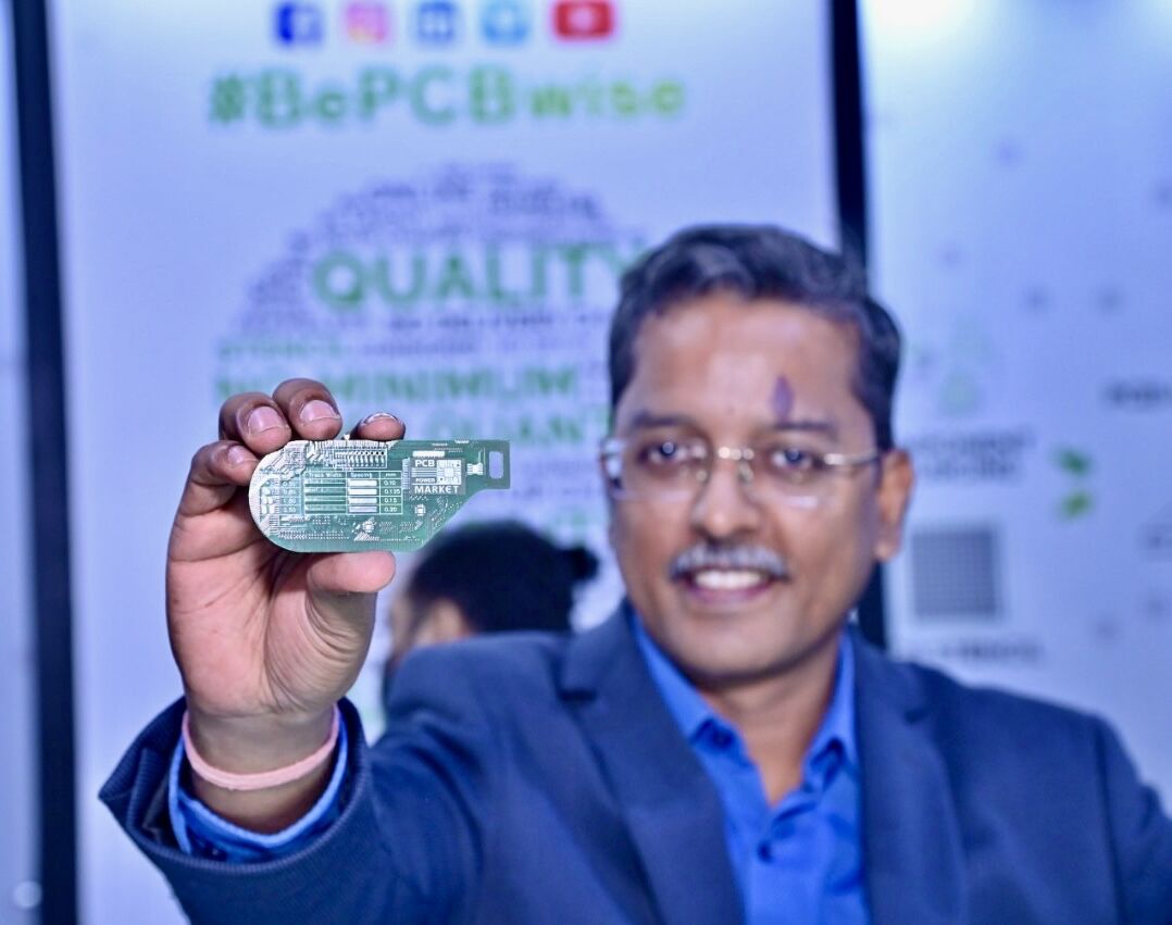
This is the most innovative visiting card I have ever received from #bePCBwise yesterday at India Expo Mart, Greater Noida in a day full of innovation | RFID | Semiconductor | Smart Tech | IOT & AI-ML


CAD data exchange is a modality of data exchange used to translate data between different Computer-aided design (CAD) authoring systems or between CAD and other downstream CAx systems. #didyouknow #bePCBwise #printedcircuitboard #Breakout #CAD #pcbpowerinc #design

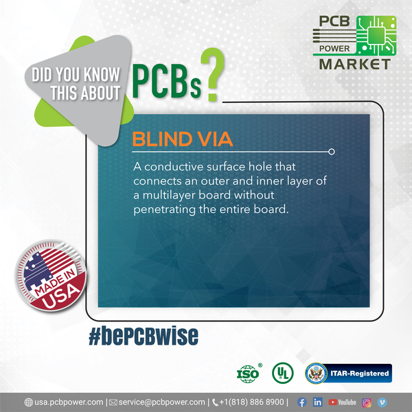
Additional Benefit of Blind Vias: Ability to widen BGA breakout channel (layer count reduction) #bePCBwise #printedcircuitboard #didyouknow #pcbpowerinc
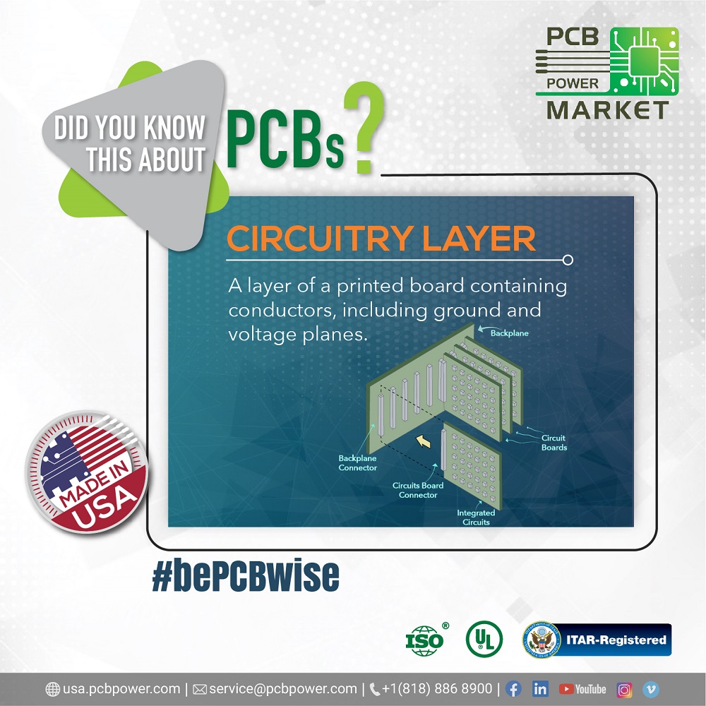
Ground plane & voltage plane together create a large parallel plate, containing conductors is called circuitry layer. #didyouknow #bePCBwise #printedcircuitboard #circuitrylayer #pcbpowerinc
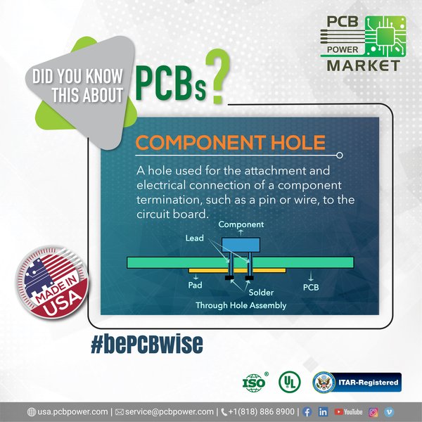
Component Holes are drills for wired components used with Through-Hole Technology. In double-sided or multilayer boards the holes will be plated through. #didyouknow #bePCBwise #printedcircuitboard #componenthole #pcbpowerinc #component
Buried Vias are used to connect between layers of a PCB where space is at a premium. It Also connects an outer layer to one or more inner layers but does not go through the entire board. #didyouknow #bePCBwise #printedcircuitboard #BuriedVia #pcbpowerinc


Here's a glimpse into the unboxing of our first ever PCB! 📦 We would like to thank PCB POWER MARKET INDIA for providing us with this custom printed circuit board!🚀 #ToDecipherUnimaginable #bepcbwise #technews #space #research #innovation #students #design #rovers #mars #tech
Team DJS Antariksh would like to thank PCB Power Market India for providing us with the most premium PCBs for our prototype Martian Rover!💯 We look forward to being associated with them!🤝 #bepcbwise #ToDecipherUnimaginable #science #partner #technology #pcb #space #engineers
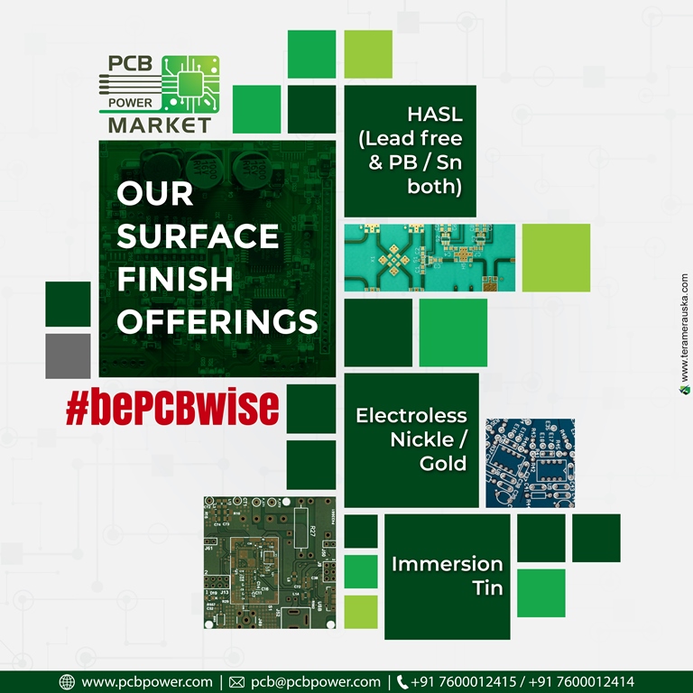
Looking for a Particular Surface Finish for your circuit board ? PCB Power Market delivers special finishes and coatings. Order today @ pcbpower.com #bePCBwise #MakeInIndia #PCBPowerMarket #PCBAssembly #PCBManufacturing #pcbdesign #pcb #printedcircuitboard
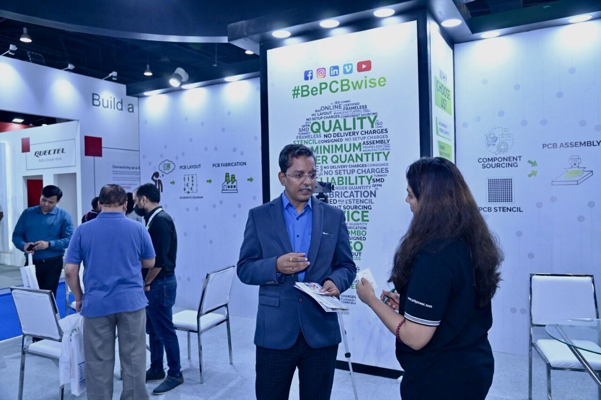
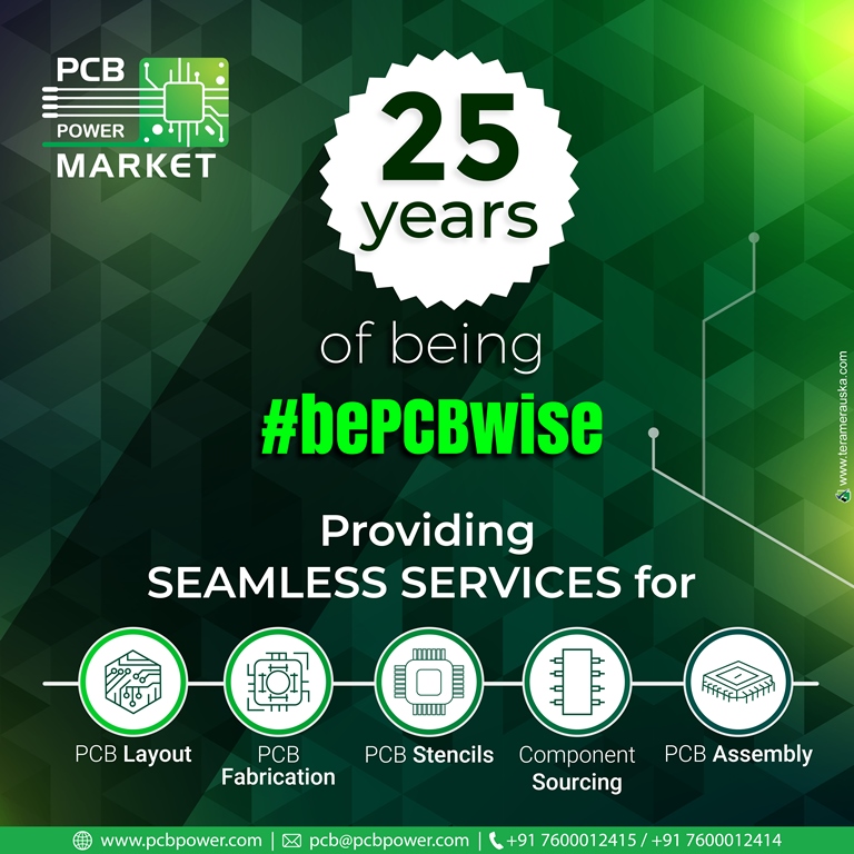
Be Wise, Be PCB Wise! With our 25 years of experience in PCB Manufacturing and Services, we are confidently catering to the Indian Businesses by delivering best PCB's Order Today with PCB Power Market pcbpower.com #bePCBwise #MakeInIndia #PCBPowerMarket #PCBAssembly
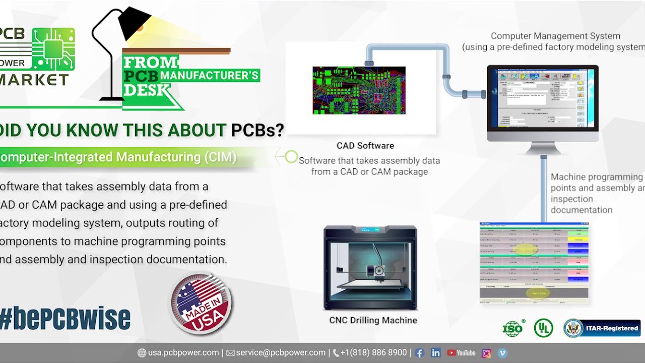
Computer-integrated manufacturing (CIM) is the use of computer technologies to integrate manufacturing activities. It contains all the functions necessary to convert the needs of the customer into the final product. youtu.be/zj3_t4rmI9w #pcbpowerinc #didyouknow #bePCBwise
youtube.com
YouTube
CIM is the use of computer technologies to integrate manufacturing...
Know how to get your data package right? Stay Connected, Stay Updated, Stay Wise. youtu.be/8sRNvD3sZqg #pcbpowermarket #bePCBwise #onlinepcb #makeinindia #pcbdesign #datapackage
youtube.com
YouTube
Know how to get your data package right?
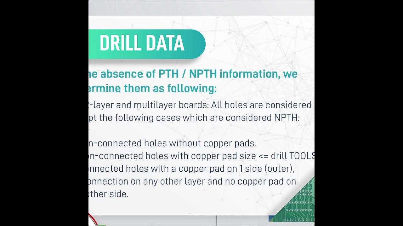
#bePCBwise How to give your Drill Data? #MakeInIndia #SupportMakeInIndia #pcbmanufacturers #electronics #pcbelectronics #pcbdesigners #PCBPowerMarket #pcbassembly #pcbmanufacturing #pcbdesign #pcb #printedcircuitboard #electricalengineering youtu.be/jMOE-39D_YY via @YouTube
youtube.com
YouTube
#bePCBwise How to give your Drill Data?
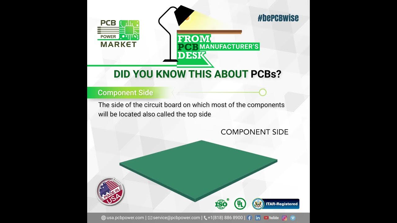
The top side of the PCB is usually the side where the components are placed and therefore sometimes also called COMPONENT SIDE. youtu.be/SJJJz45oNy8 #didyouknow #bePCBwise #printedcircuitboard #componenthole #pcbpowerinc #componentside
youtube.com
YouTube
The top side of the PCB is the side where the components are placed...
The copper area on a PCB surface or on the internal layer is mainly composed of pads, the part of the PCB to which component leads are connected and paths also known as traces. youtu.be/gugHJ4CigBs #PCBSurface #bePCBwise #component #printedcircuitboard #pcbpowerinc
DJS Antariksh is very pleased to announce @PCBPowerInc as our Official PCB Partner! 🤝 PCB Power Market India have succeeded in bringing the idea of an integrated PCB excellence platform to life, with equal impetus on customer-centricity and sustained growth. 💯 #bepcbwise
This is the most innovative visiting card I have ever received from #bePCBwise yesterday at India Expo Mart, Greater Noida in a day full of innovation | RFID | Semiconductor | Smart Tech | IOT & AI-ML
Team DJS Antariksh would like to thank PCB Power Market India for providing us with the most premium PCBs for our prototype Martian Rover!💯 We look forward to being associated with them!🤝 #bepcbwise #ToDecipherUnimaginable #science #partner #technology #pcb #space #engineers
Here's a glimpse into the unboxing of our first ever PCB! 📦 We would like to thank PCB POWER MARKET INDIA for providing us with this custom printed circuit board!🚀 #ToDecipherUnimaginable #bepcbwise #technews #space #research #innovation #students #design #rovers #mars #tech
DJS Antariksh is very pleased to announce @PCBPowerInc as our Official PCB Partner! 🤝 PCB Power Market India have succeeded in bringing the idea of an integrated PCB excellence platform to life, with equal impetus on customer-centricity and sustained growth. 💯 #bepcbwise
#bePCBwise How to give your Drill Data? #MakeInIndia #SupportMakeInIndia #pcbmanufacturers #electronics #pcbelectronics #pcbdesigners #PCBPowerMarket #pcbassembly #pcbmanufacturing #pcbdesign #pcb #printedcircuitboard #electricalengineering youtu.be/jMOE-39D_YY via @YouTube
youtube.com
YouTube
#bePCBwise How to give your Drill Data?
Looking for a Particular Surface Finish for your circuit board ? PCB Power Market delivers special finishes and coatings. Order today @ pcbpower.com #bePCBwise #MakeInIndia #PCBPowerMarket #PCBAssembly #PCBManufacturing #pcbdesign #pcb #printedcircuitboard
Be Wise, Be PCB Wise! With our 25 years of experience in PCB Manufacturing and Services, we are confidently catering to the Indian Businesses by delivering best PCB's Order Today with PCB Power Market pcbpower.com #bePCBwise #MakeInIndia #PCBPowerMarket #PCBAssembly
The copper area on a PCB surface or on the internal layer is mainly composed of pads, the part of the PCB to which component leads are connected and paths also known as traces. youtu.be/gugHJ4CigBs #PCBSurface #bePCBwise #component #printedcircuitboard #pcbpowerinc
If the copper plate behaves like the skeleton of the PCB, acting as its primary structure - then the components are the vital organs. Each one has a different function. They give the circuit the unique qualities that make it fit for its intended purpose. #didyouknow #bePCBwise
This is the most innovative visiting card I have ever received from #bePCBwise yesterday at India Expo Mart, Greater Noida in a day full of innovation | RFID | Semiconductor | Smart Tech | IOT & AI-ML
CAD data exchange is a modality of data exchange used to translate data between different Computer-aided design (CAD) authoring systems or between CAD and other downstream CAx systems. #didyouknow #bePCBwise #printedcircuitboard #Breakout #CAD #pcbpowerinc #design
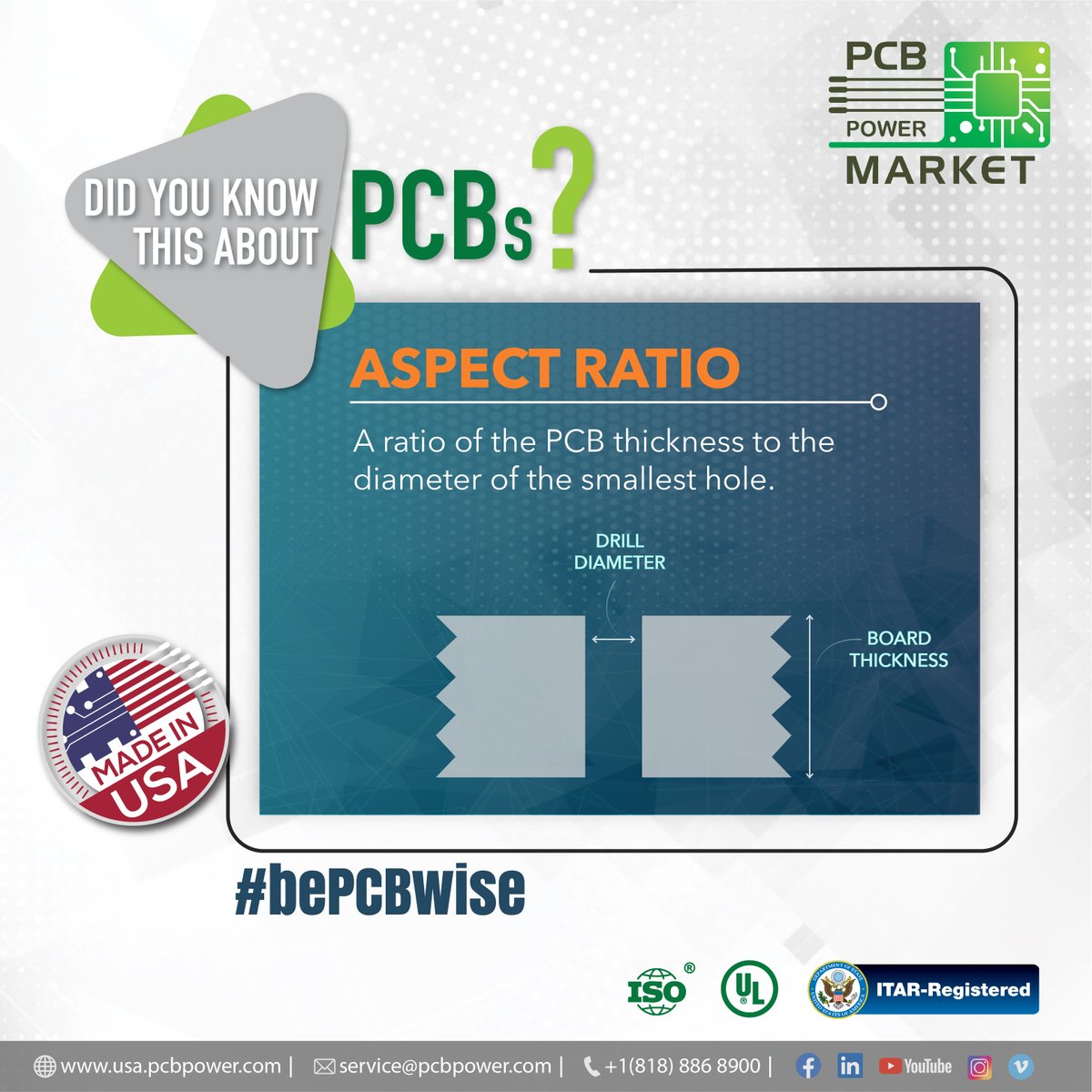
The aspect ratio is the thickness of a PCB divided by the diameter size of a drilled hole. #bePCBwise #printedcircuitboard #didyouknow #aspectratio #pcb #pcbpowermarket
Additional Benefit of Blind Vias: Ability to widen BGA breakout channel (layer count reduction) #bePCBwise #printedcircuitboard #didyouknow #pcbpowerinc
A ball grid array (BGA) is a type of surface-mount packaging (a chip carrier) used for integrated circuits. #bePCBwise #printedcircuitboard #BallGridArray #pcbpowermarket #didyouknow #knowledge

The basic concept of a breakout board that takes a single electrical component and makes it easy to use. #didyouknow #bePCBwise #printedcircuitboard #Breakout #pcbpowerinc

Automated optical inspection i.e. AOI is responsible for quality control for both PCB manufacturing and PCB assembly. #bePCBwise #pcb #AOI #pcbassembly #pcbmanufacturing

Ground plane & voltage plane together create a large parallel plate, containing conductors is called circuitry layer. #didyouknow #bePCBwise #printedcircuitboard #circuitrylayer #pcbpowerinc
The thickness of the base metal is an important essential variable when performing weld overlays, because the thicker the base metal, the generally the weaker it is. #pcbdesign #bePCBwise #printedcircuitboard #didyouknow #knowledge #pcbpowermarket

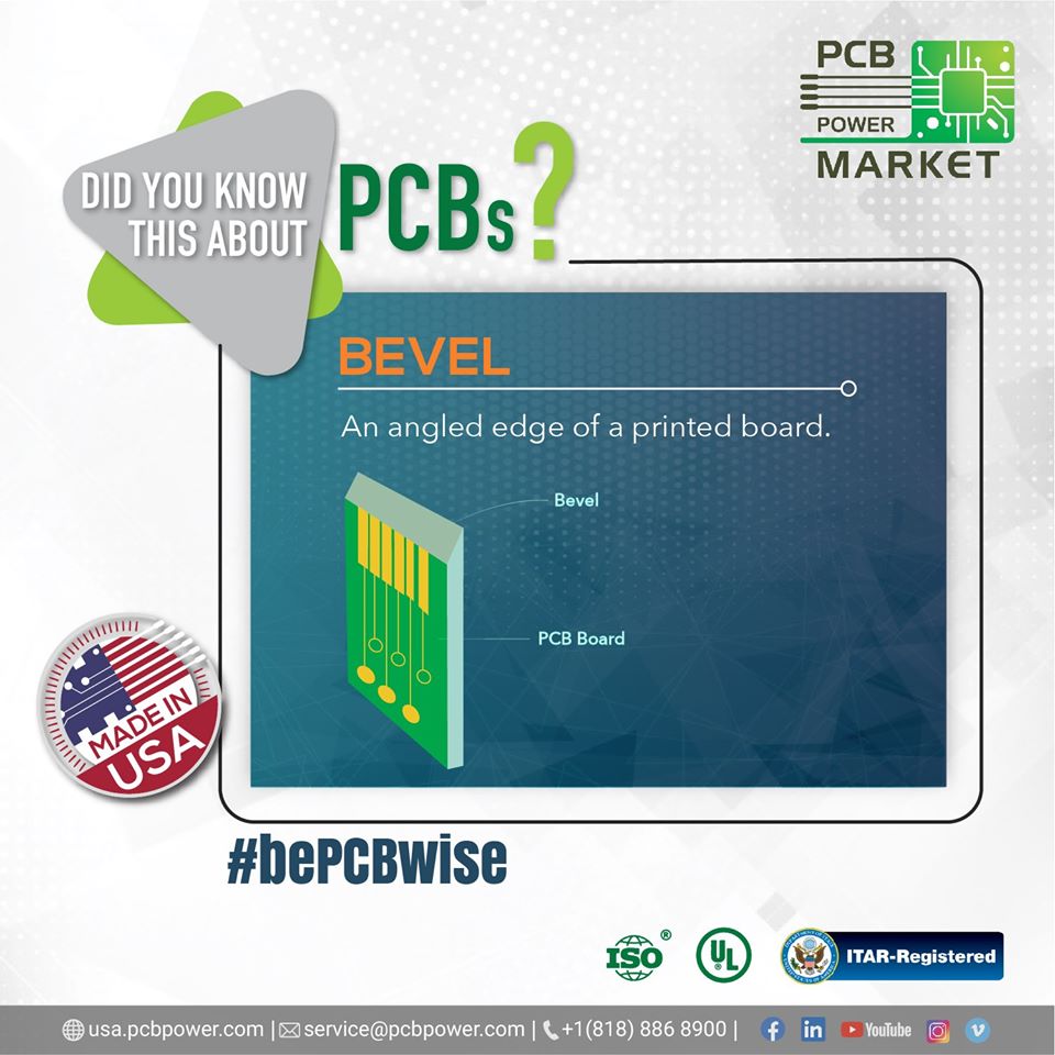
A bevel is typically used to soften the edge of a piece for the sake of safety, wear resistance, aesthetics or to facilitate mating with another piece. #bePCBwise #printedcircuitboard #didyouknow #pcbpowerinc #bevel
Component Holes are drills for wired components used with Through-Hole Technology. In double-sided or multilayer boards the holes will be plated through. #didyouknow #bePCBwise #printedcircuitboard #componenthole #pcbpowerinc #component
PCBs manufacturing process starts with a dielectric material with copper on both sides. This base copper is described by its weight evenly spread over one square foot. #bePCBwise #printedcircuitboard #pcbpowermarket #basecopper #didyouknow #knowledge

Buried Vias are used to connect between layers of a PCB where space is at a premium. It Also connects an outer layer to one or more inner layers but does not go through the entire board. #didyouknow #bePCBwise #printedcircuitboard #BuriedVia #pcbpowerinc
Looking for a Particular Surface Finish for your circuit board ? PCB Power Market delivers special finishes and coatings. Order today @ pcbpower.com #bePCBwise #MakeInIndia #PCBPowerMarket #PCBAssembly #PCBManufacturing #pcbdesign #pcb #printedcircuitboard
Be Wise, Be PCB Wise! With our 25 years of experience in PCB Manufacturing and Services, we are confidently catering to the Indian Businesses by delivering best PCB's Order Today with PCB Power Market pcbpower.com #bePCBwise #MakeInIndia #PCBPowerMarket #PCBAssembly
Something went wrong.
Something went wrong.
United States Trends
- 1. #BaddiesUSA 60.8K posts
- 2. Rams 29.4K posts
- 3. #LAShortnSweet 21.7K posts
- 4. TOP CALL 3,343 posts
- 5. Scotty 9,841 posts
- 6. Cowboys 101K posts
- 7. Eagles 141K posts
- 8. Chip Kelly 8,724 posts
- 9. #TROLLBOY 1,986 posts
- 10. sabrina 61.5K posts
- 11. #ITWelcomeToDerry 15.6K posts
- 12. Raiders 67.7K posts
- 13. #centralwOrldXmasXFreenBecky 245K posts
- 14. Stacey 24.4K posts
- 15. SAROCHA REBECCA DISNEY AT CTW 257K posts
- 16. Stafford 15.2K posts
- 17. Ahna 7,271 posts
- 18. Bucs 12.3K posts
- 19. Baker 20.8K posts
- 20. Market Focus 2,200 posts