#waferprocessing search results

What We’re Looking For Experience operating semiconductor equipment, including grinding and drilling processes, machine setup, parameter tuning, and basic process adjustments. #ProcessEngineering #WaferProcessing #PrecisionMachining

📧 [email protected] 🌐 fyyschemistry.com 📱 WhatsApp. +86 18149115649 #SemiconductorMaterials #ChamberCleaning #WaferProcessing #GuanidineCarbonate #CleaningChemistry #CVDcleaning #WetCleaning #ProcessChemicals #YieldImprovement


Chemical Mechanical Planarization (CMP) Slurry Market is set to reach USD 854.3 Million by 2032, up from USD 525.62 Million in 2024, growing at a CAGR of 6.3% (2025–2032). consegicbusinessintelligence.com/chemical-mecha… #CMPSlurry #SemiconductorMaterials #WaferProcessing #SemiconductorMarket


Be our guest at #SEMICONWest with a FREE one-day expo pass: bit.ly/ECM-SEMI24 📅 SEMICON West | San Francisco | July 9-11 📌 BOOTH 259 ECM GREENTECH / Wafer Processing Furnaces ANNEALSYS / RTP & DLI-CVD SEMCO TECH / Gas Components & ESCs #semiconductor #waferprocessing

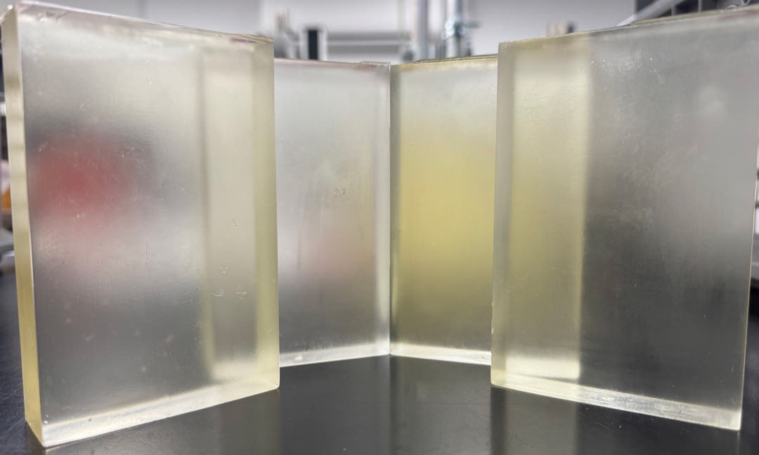
Tokyo Electron Trias CVD High K Process Module. Retired from frontline fabs—perfect for R&D, pilot lines, or legacy nodes. Send us message to make an offer. #TokyoElectron #CVD #WaferProcessing #FabTools #ChipMaking #Visionsemiconductorsolutions

Wafer grinder market is projected to reach $1,235 million in 2035, from $710 million in 2024, witnessing a CAGR of 5.9% during the forecast period (2025-2035). For more details:bit.ly/4bIrsM0 #WaferGrinder #SemiconductorManufacturing #WaferProcessing #WaferThinning


Thin Wafer Processing and Dicing Equipment Market Outlook, Size and Analysis 2034 marketresearchfuture.com/reports/thin-w… #WaferProcessing #SemiconductorDicing #ThinWaferTech #ChipFabrication #Microelectronics
marketresearchfuture.com
Thin Wafer Processing and Dicing Equipment Market Outlook, Size and Analysis 2035
Thin Wafer Processing Dicing Equipment Market will grow at 5.48% CAGR, reaching $3.72 Billion by 2035 | advancements in semiconductor technology and increasing demand for miniaturized devices.

🔬 In #semiconductors, there's no room for error. We engineer high-precision #polyurethane components—like wire saw rollers & pulleys—to boost wafer slicing performance, durability & uptime. 💡Let’s talk custom solutions: bit.ly/42Fi60L #WaferProcessing #Manufacturing

Wafer Backgrinding Tape Market Size, Share Report and Growth 2034 #WaferProcessing #SemiconductorMaterials #BackgrindingTape #ChipManufacturing marketresearchfuture.com/reports/wafer-…
marketresearchfuture.com
Wafer Backgrinding Tape Market Size, Share Report and Growth 2035
Wafer Backgrinding Tape Market is expected to grow USD 4.65 Billion at 7.32% CAGR by 2035, Global Wafer Backgrinding Tape Industry Analysis by Application, Tape Type, Material, End Use Industry,...
Photoresist Stripper Market Size, Share Report and Industry 2034 marketresearchfuture.com/reports/photor… #PhotoresistStripper #SemiconductorCleaning #WaferProcessing #LithographyChemicals #ChipManufacturing
marketresearchfuture.com
Photoresist Stripper Market Size, Share Report and Industry 2035
Photoresist Stripper Market is predicted to register a CAGR of 5.32% to reach USD 5.56 Billion by 2035, Global Photoresist Stripper Industry Analysis By Application, Technology, Chemical Type, End...
Diffusion Equipment Market Size, Share, Trends and Growth 2034 marketresearchfuture.com/reports/diffus… #DiffusionEquipment #SemiconductorManufacturing #WaferProcessing #ElectronicsIndustry #FabEquipment
marketresearchfuture.com
Diffusion Equipment Market Size, Share, Trends and Growth 2035
Diffusion Equipment Market is predicted to register a CAGR of 5.80% to reach USD 2.64 Billion by 2035, Global Diffusion Equipment Market Growth by Type, Application | Diffusion Equipment Industry

Dielectric Etcher Market Share Analysis, Sales Revenue, Competitive Landscape and Market Expansion Strategies 2035 marketresearchfuture.com/reports/dielec… #SemiconductorEquipment #WaferProcessing #ChipManufacturing
marketresearchfuture.com
Dielectric Etcher Market Size, Share, Trends Forecast 2035
Dielectric Etcher Market is Expected to Reach a Valuation of $ 6.95B by 2035, Growing at a CAGR of 5.48% During 2025 - 2035 | Blockchain Technology Integration

⏰ The deadlines for this year's multi-project wafer runs are soon. Have you submitted your designs yet? Our PDKs are free and available via @Synopsys, Nazca, and @lucedaphotonics, with packaging available! lionix-international.com/photonics/mpw-… #MPW #SiliconPhotonics #WaferProcessing

ECM Greentech | Annealsys | Semco Technologies 📍 Booth 259 @ SEMICON West, July 9-11th #SEMICONWest is next week! Visit the link below for FREE one-day access to the exhibit hall or a discount on other packages. #semiconductor #waferprocessing semi24.nvytes.co/semi24inv/259.…


💡반도체 제조 장비 시장 급성장! 📈2023년 110.9B → 2032년 270.3B 달성 전망 🌏아시아태평양이 67.89% 점유로 선도! 🚀 웨이퍼·IC칩·메모리 생산 자동화 수요가 핵심 성장 동력! #반도체장비 #Semiconductor #WaferProcessing #포토리소그래피 업 🔗 fortunebusinessinsights.com/ko/semiconduct…

THIS WEEK | CS MANTECH | Tucson, AZ ECM (Booth 499) & ANNEALSYS (Booth 400) are in Tucson, AZ at CS MANTECH ready to discuss how our #waferprocessing furnaces can optimize your #semiconductor manufacturing process (ATMO, SAPCVD, LPCVD, RTP, RTA, RTN,...) ecm-usa.com/greentech


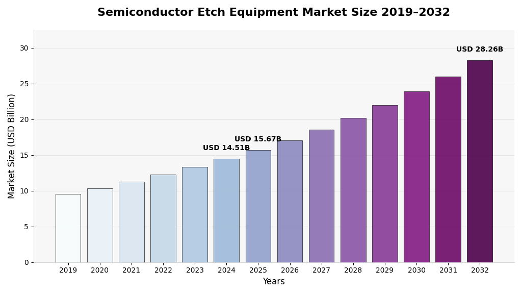
Global Semiconductor Etch Equipment Market 2024: USD 14.51 Billion 2025: USD 15.67 Billion 2032: USD 28.26 Billion 📈 CAGR: 8.8% (2025–2032) 🌏 Asia Pacific Share (2023): 61.69% 🔗fortunebusinessinsights.com/semiconductor-… #Semiconductor #EtchEquipment #WaferProcessing #MarketResearch
Semiconductor Etch Equipment Market Size, Share & Trends 2035 #SemiconductorEtch #WaferProcessing #EtchEquipment #SemiconductorManufacturing marketresearchfuture.com/reports/semico…
marketresearchfuture.com
Semiconductor Etch Equipment Market Size, Share & Trends 2035
Semiconductor Etch Equipment Market is predicted to grow at 6.32% CAGR from 2025 to 2035, Semiconductor Etch Equipment Industry Analysis by Technology, Type, End Use Industry, Application and Region
Diffusion Equipment Market Trends Analysis, Sales Revenue, Competitive Landscape and Market Expansion Strategies 2035 marketresearchfuture.com/reports/diffus… #DiffusionEquipment #SemiconductorManufacturing #WaferProcessing #ChipFabrication
marketresearchfuture.com
Diffusion Equipment Market Size, Share, Trends and Growth 2035
Diffusion Equipment Market is predicted to register a CAGR of 5.80% to reach USD 2.64 Billion by 2035, Global Diffusion Equipment Market Growth by Type, Application | Diffusion Equipment Industry

Semiconductor Wafer Polishing Grinding Equipment Market Share Analysis, Sales Revenue, Competitive Landscape and Market Expansion Strategies 2035 marketresearchfuture.com/reports/semico… #SemiconductorEquipment #WaferProcessing #ChipManufacturing
marketresearchfuture.com
Semiconductor Wafer Polishing Grinding Equipment Market Size, Share 2035
Semiconductor Wafer Polishing and Grinding Equipment Market is predicted to reach USD 7.21 Billion at CAGR 3.84% by 2035, Semiconductor Wafer Polishing and Grinding Equipment Industry Growth by...

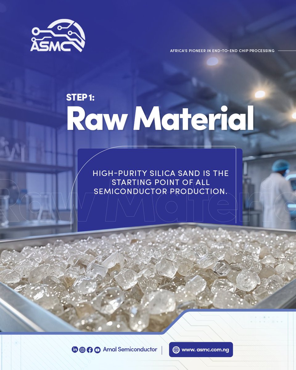
Wafer Processing: Transforming raw materials into the canvas for digital innovation. Discover how ASMC is powering the future of semiconductor technology. #ASMC #waferprocessing #semiconductorinnovation #siliconwafers #madeinnigeria #techinafrica #africaninnovation


Tokyo Electron Trias CVD High K Process Module. Retired from frontline fabs—perfect for R&D, pilot lines, or legacy nodes. Send us message to make an offer. #TokyoElectron #CVD #WaferProcessing #FabTools #ChipMaking #Visionsemiconductorsolutions

Anturit: Modernin teknologian digitaaliset silmät ja korvat - Tech amaletejas.blogaaja.fi/2025/07/17/ant… #SemiconductorFoundry #ChipManufacturing #WaferProcessing #SemiconductorMarket #Microelectronics #FutureOfChips
Discussion - My Site Group | thekawa thekawa.org/group/my-site-… #SemiconductorFoundry #ChipManufacturing #WaferProcessing #SemiconductorMarket #Microelectronics #FutureOfChips #ChipProduction #ElectronicsIndustry

Flow Control In Semiconductor Market Size, Share & Trends Report 2035 marketresearchfuture.com/reports/flow-c… #SemiconductorFlowControl #WaferProcessing #GasFlowControl #ChipManufacturing #FabTechnology
Radiation Hardened Electronics Semiconductor Market Report, Size and Growth 2034 marketresearchfuture.com/reports/radiat… #PhotoresistStripper #SemiconductorCleaning #WaferProcessing #LithographyChemicals #ChipManufacturing
marketresearchfuture.com
Radiation Hardened Electronics Semiconductor Market Size, Share | Report [2035]
Radiation Hardened Electronics Semiconductor Market is expected to grow at 4.85% CAGR, reaching USD 6.04 Billion by 2035, driven by increasing demand in aerospace, defense, and space exploration.
Photoresist Stripper Market Size, Share Report and Industry 2034 marketresearchfuture.com/reports/photor… #PhotoresistStripper #SemiconductorCleaning #WaferProcessing #LithographyChemicals #ChipManufacturing
marketresearchfuture.com
Photoresist Stripper Market Size, Share Report and Industry 2035
Photoresist Stripper Market is predicted to register a CAGR of 5.32% to reach USD 5.56 Billion by 2035, Global Photoresist Stripper Industry Analysis By Application, Technology, Chemical Type, End...
Thin Wafer Processing and Dicing Equipment Market Outlook, Size and Analysis 2034 marketresearchfuture.com/reports/thin-w… #WaferProcessing #SemiconductorDicing #ThinWaferTech #ChipFabrication #Microelectronics
marketresearchfuture.com
Thin Wafer Processing and Dicing Equipment Market Outlook, Size and Analysis 2035
Thin Wafer Processing Dicing Equipment Market will grow at 5.48% CAGR, reaching $3.72 Billion by 2035 | advancements in semiconductor technology and increasing demand for miniaturized devices.
Wafer Backgrinding Tape Market Size, Share Report and Growth 2034 #WaferProcessing #SemiconductorMaterials #BackgrindingTape #ChipManufacturing marketresearchfuture.com/reports/wafer-…
marketresearchfuture.com
Wafer Backgrinding Tape Market Size, Share Report and Growth 2035
Wafer Backgrinding Tape Market is expected to grow USD 4.65 Billion at 7.32% CAGR by 2035, Global Wafer Backgrinding Tape Industry Analysis by Application, Tape Type, Material, End Use Industry,...
Semiconductor Etch Equipment Market Size, Share & Trends 2035 #SemiconductorEtch #WaferProcessing #EtchEquipment #SemiconductorManufacturing marketresearchfuture.com/reports/semico…
marketresearchfuture.com
Semiconductor Etch Equipment Market Size, Share & Trends 2035
Semiconductor Etch Equipment Market is predicted to grow at 6.32% CAGR from 2025 to 2035, Semiconductor Etch Equipment Industry Analysis by Technology, Type, End Use Industry, Application and Region
📧 [email protected] 🌐 fyyschemistry.com 📱 WhatsApp. +86 18149115649 #SemiconductorMaterials #ChamberCleaning #WaferProcessing #GuanidineCarbonate #CleaningChemistry #CVDcleaning #WetCleaning #ProcessChemicals #YieldImprovement

Lithography: The Art Behind the Chip At the heart of every semiconductor lies the power of lithography — enabling intricate micro and nano-scale patterning on wafers with unmatched accuracy. #SemiconductorTech #Lithography #WaferProcessing #Microelectronics #RRPElectronics


Diffusion Equipment Market Size, Share, Trends and Growth 2034 #DiffusionEquipment #SemiconductorEquipment #WaferProcessing #CleanroomTech marketresearchfuture.com/reports/diffus…
marketresearchfuture.com
Diffusion Equipment Market Size, Share, Trends and Growth 2035
Diffusion Equipment Market is predicted to register a CAGR of 5.80% to reach USD 2.64 Billion by 2035, Global Diffusion Equipment Market Growth by Type, Application | Diffusion Equipment Industry

Did you know? 🤔 The Front-End process in semiconductor manufacturing builds the tiny circuits on silicon wafers before chips are packaged! It all happens in ultra-clean rooms 👌 #Semiconductor #WaferProcessing #FrontEnd #TechFacts


We’re heading to @csmantech in a few weeks! Stop by booth 512 to discover the power of the Solstice® platform. Let’s connect: [email protected] #Semiconductors #WaferProcessing

🔬 In #semiconductors, there's no room for error. We engineer high-precision #polyurethane components—like wire saw rollers & pulleys—to boost wafer slicing performance, durability & uptime. 💡Let’s talk custom solutions: bit.ly/42Fi60L #WaferProcessing #Manufacturing
Wafer grinder market is projected to reach $1,235 million in 2035, from $710 million in 2024, witnessing a CAGR of 5.9% during the forecast period (2025-2035). For more details:bit.ly/4bIrsM0 #WaferGrinder #SemiconductorManufacturing #WaferProcessing #WaferThinning

#OMRON offers a range of detection methods that allow engineers to accurately locate the #wafer notch. That's one of the reasons why OMRON sensing solutions are a standard in front end #waferprocessing during #semiconductor manufacturing. Find out more: omron.pub/3D7MDdP


THREAD🧵 💡Analyse équipementier semi-conducteurs, zoom sur la société KLA-Corp $KLAC 📱 ➡️KLA propose des équipements de contrôle du processus de fabrication des semi-conducteurs. #waferprocessing #SP500 #Bourse 👇Keep Locking Ahead ! 1/11


The countdown to our Founder's Day continues with our #FlashbackFriday series! 💥 The CLEAN TRACK system debuted in 1982, setting new standards in wafer processing! Compact, powerful, and efficient – a game-changer for semiconductors. 🌟 #WaferProcessing #TechEdition

📧 [email protected] 🌐 fyyschemistry.com 📱 WhatsApp. +86 18149115649 #SemiconductorMaterials #ChamberCleaning #WaferProcessing #GuanidineCarbonate #CleaningChemistry #CVDcleaning #WetCleaning #ProcessChemicals #YieldImprovement
ECM Greentech | Annealsys | Semco Technologies 📍 Booth 259 @ SEMICON West, July 9-11th #SEMICONWest is next week! Visit the link below for FREE one-day access to the exhibit hall or a discount on other packages. #semiconductor #waferprocessing semi24.nvytes.co/semi24inv/259.…
Wafer grinder market is projected to reach $1,235 million in 2035, from $710 million in 2024, witnessing a CAGR of 5.9% during the forecast period (2025-2035). For more details:bit.ly/4bIrsM0 #WaferGrinder #SemiconductorManufacturing #WaferProcessing #WaferThinning
🔬 In #semiconductors, there's no room for error. We engineer high-precision #polyurethane components—like wire saw rollers & pulleys—to boost wafer slicing performance, durability & uptime. 💡Let’s talk custom solutions: bit.ly/42Fi60L #WaferProcessing #Manufacturing
💡반도체 제조 장비 시장 급성장! 📈2023년 110.9B → 2032년 270.3B 달성 전망 🌏아시아태평양이 67.89% 점유로 선도! 🚀 웨이퍼·IC칩·메모리 생산 자동화 수요가 핵심 성장 동력! #반도체장비 #Semiconductor #WaferProcessing #포토리소그래피 업 🔗 fortunebusinessinsights.com/ko/semiconduct…

Learn how to make your products cost-effective and designed for manufacture through the help of this updated detailed guide. hubs.ly/Q023kryM0 #Semiconductor #SemiconductorIndustry #WaferProcessing

THREAD🧵 💡Analyse équipementier semi-conducteurs, zoom sur la société KLA-Corp $KLAC 📱 ➡️KLA propose des équipements de contrôle du processus de fabrication des semi-conducteurs. #waferprocessing #SP500 #Bourse 👇Keep Locking Ahead ! 1/11
THIS WEEK | CS MANTECH | Tucson, AZ ECM (Booth 499) & ANNEALSYS (Booth 400) are in Tucson, AZ at CS MANTECH ready to discuss how our #waferprocessing furnaces can optimize your #semiconductor manufacturing process (ATMO, SAPCVD, LPCVD, RTP, RTA, RTN,...) ecm-usa.com/greentech

Disco invests 40B yen in a new Hiroshima plant, boosting wafer processing to meet rising semiconductor demand. Source: shorturl.at/kpvSX #DiscoExpansion #SemiconductorSurge #WaferProcessing #TechFuture

⏰ The deadlines for this year's multi-project wafer runs are soon. Have you submitted your designs yet? Our PDKs are free and available via @Synopsys, Nazca, and @lucedaphotonics, with packaging available! lionix-international.com/photonics/mpw-… #MPW #SiliconPhotonics #WaferProcessing
Meet with our ECM Greentech & @ANNEALSYS teams this week at ICSCRM 2024 in Raleigh, NC to find the best R&D or production equipment for your #sicgrowth #semiconductor #waferprocessing applications! 📆 September 29 - October 4 📍 BOOTH 62 bit.ly/ecm-lab

Global Semiconductor Etch Equipment Market 2024: USD 14.51 Billion 2025: USD 15.67 Billion 2032: USD 28.26 Billion 📈 CAGR: 8.8% (2025–2032) 🌏 Asia Pacific Share (2023): 61.69% 🔗fortunebusinessinsights.com/semiconductor-… #Semiconductor #EtchEquipment #WaferProcessing #MarketResearch
The countdown to our Founder's Day continues with our #FlashbackFriday series! 💥 The CLEAN TRACK system debuted in 1982, setting new standards in wafer processing! Compact, powerful, and efficient – a game-changer for semiconductors. 🌟 #WaferProcessing #TechEdition
Wafer Processing: Transforming raw materials into the canvas for digital innovation. Discover how ASMC is powering the future of semiconductor technology. #ASMC #waferprocessing #semiconductorinnovation #siliconwafers #madeinnigeria #techinafrica #africaninnovation

Disco invests 40B yen in a new Hiroshima plant, boosting wafer processing to meet rising semiconductor demand. Source: shorturl.at/kpvSX #DiscoExpansion #SemiconductorSurge #WaferProcessing #TechFuture

Chemical Mechanical Planarization (CMP) Slurry Market is set to reach USD 854.3 Million by 2032, up from USD 525.62 Million in 2024, growing at a CAGR of 6.3% (2025–2032). consegicbusinessintelligence.com/chemical-mecha… #CMPSlurry #SemiconductorMaterials #WaferProcessing #SemiconductorMarket
Lithography: The Art Behind the Chip At the heart of every semiconductor lies the power of lithography — enabling intricate micro and nano-scale patterning on wafers with unmatched accuracy. #SemiconductorTech #Lithography #WaferProcessing #Microelectronics #RRPElectronics
Something went wrong.
Something went wrong.
United States Trends
- 1. Chris Murphy N/A
- 2. Splatoon Raiders N/A
- 3. Good Tuesday N/A
- 4. #MachadoYBauteRacistas N/A
- 5. Vote NO N/A
- 6. CNBC N/A
- 7. Thune N/A
- 8. US Senator N/A
- 9. #GuardNIKKEStars N/A
- 10. Battle of San Jacinto N/A
- 11. Nuns N/A
- 12. #pilotstwtselfieday N/A
- 13. Rocki N/A
- 14. Alan Osmond N/A
- 15. #NMIXX N/A
- 16. $UNH N/A
- 17. #TacoTuesday N/A
- 18. Happy Taco N/A
- 19. kevin warsh N/A
- 20. Brake N/A