#euv search results

🚀 New #TSMC roadmap alert! The foundry giant unveiled A12 (1.2nm) and A13 (1.3nm), both targeting 2029 — and notably, neither is expected to require ASML’s High-NA #EUV. A pointed contrast to #Intel's 14A strategy. 💡More: pse.is/8yuzfd 🔗


Intel's upcoming 14A process node will be more expensive than its predecessor due to the use of advanced high-NA EUV lithography machines. #Intel #14A #EUV #Semiconductors #TechNews securityonline.info/intels-14a-pro…

How US sanctions backfired: China EUV lithography tech breakthrough! #US #EUV #China #ai #chips #chn #lithography #semiconductor #inn #光刻机 @TechweekInc #tech #cn YouTube: youtu.be/AJRpNbmmivU

❗China has secretly built a prototype of a cutting-edge chip-making machine (#EUV lithography) in Shenzhen. It was built by former engineers at the Dutch company ASML. The machine is already producing the special light it needs, but it can’t yet make working chips, per @Reuters.

China Invests €37 Billion to Develop Domestic #EUV #Lithography Systems #semiconductor #manufacturing powerelectronicsnews.com/china-invests-…

🔥 While TSMC reportedly upgrades Kumamoto Fab 2 to 3nm, #Samsung is quietly moving ahead in #Taylor—said to have secured partial use approvals, with #EUV tests planned as early as next month.💡More: pse.is/8pa5wq 🔗
trendforce.com
[News] Samsung Reportedly Secures Partial Taylor Fab Use Approval, Timeline May Move Up
Samsung’ Taylor fab is reportedly making tangible progress. Citing Korea JoongAng Daily, the report says the company has obtained temporary approval f...
Made-in-China EUV machine target AI chip output by 2028 #Tech #semiconductor #euv #Lithography #China #techs #Huawei #ai #Deepseek #ic 1️⃣ asiatimes.com/2025/12/made-i…
🤔 Is #China really closing the gap with Samsung and SK hynix? An #HBM expert says the tech divide already exceeds 5 years—and could widen further as access to #EUV remains restricted.💡More: pse.is/8p4t39 🔗
trendforce.com
[News] HBM Expert Says Korea–China Memory Gap Exceeds 5 Years and May Even Widen Amid EUV Constra...
Is China closing the gap with South Korea’s memory giants? An industry veteran says the gap may be wider than assumed. According to The Korea Herald, ...

Currently, #ASML’s revenue contribution from #EUV and #DUV isn’t that far apart. While EUV systems are primarily ordered by #TSMC, #Intel, and #Samsung, the urgency for High NA EUV isn’t quite there yet. Intel and Samsung’s 2nm mass production remains delayed, and even CC admits
Clarity..Hardwork..Result & Consistency. Proud of you ma Ranjitha. 🔥🔥🔥💐💐💐 #Congratulations #EUV #SpashtathaReview

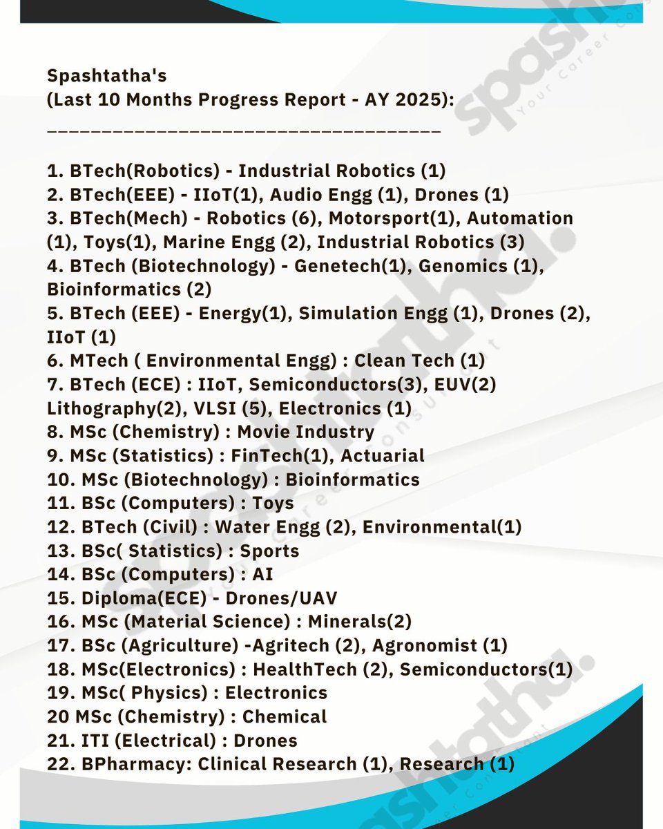
ఈ విద్యా సంవత్సరంలో గడిచిన పది నెలల్లో మా #స్పష్టత నిర్దేశకత్వంలో మా విద్యార్థులు సాధించిన నాన్ ఐటీ ప్లేస్మెంట్ సునామీ. Placement (65) Progress Card of last 10 months of 2025-26. #Congratulations To all. 🍻🔥👏 Thank-you all for making our #Spashtatha proud. #SpashtathaReview

📈 #ASML posts a record €9.7B in 4Q25 net sales on #EUV and AI momentum—but China-related revenue is expected to fall to ~20% in 2026, from 33% in 2025. 💡More: buff.ly/dTEeIC0 🔗


IBM and Lam Research expand partnership to develop High-NA #EUV processes aimed at enabling sub-1-nm chips for future #AI systems. eetimes.com/ibm-lam-resear…

మేము మార్చి నుండే మొదలు పెట్టాం.. 🔥🔥🔥 #EUV #DUV #స్పష్టత #SpashtathaReview

#ECE వైపు వద్దు..గ్రోత్ ఉండదు..నీ వల్ల కాదని ఎంతమంది నిరుత్సాహపరిచినా తాను నమ్మిన అంశం మీద 6 నెలలు కష్టపడి మా మెంటరింగ్ ద్వారా ప్రపంచవ్యాప్తంగా 1600 రాసిన పరీక్షలో ఎన్నికైన 25 మందిలో ఒకరిగా నిలచిన రజిత గారికి #స్పష్టత తరపున మనఃపూర్వక అభినందనలు. #Spashtatha #EUV #Internship

🔥 #Intel clears acceptance testing on the world’s first 2nd-gen High-NA #EUV. With #ASML reportedly eyeing 2027–28 mass production, is the foundry race about to shift?💡More: buff.ly/4Bacsg1 🔗

Bereit für Europa Universalis 5 und weitere Neuheiten in dieser Woche? Ein Überblick über wichtige Releases und unsere Sales: 🔥 gplnk.com/408387 #EuropaUniversalisV #EU5 #EUV

👀 From paper to photolithography—Oji Holdings is pushing a bio-based #EUV #photoresist targeting 2nm and beyond. What other unexpected Japanese players are quietly shaping the chip industry?💡More: pse.is/8qnckh 🔗


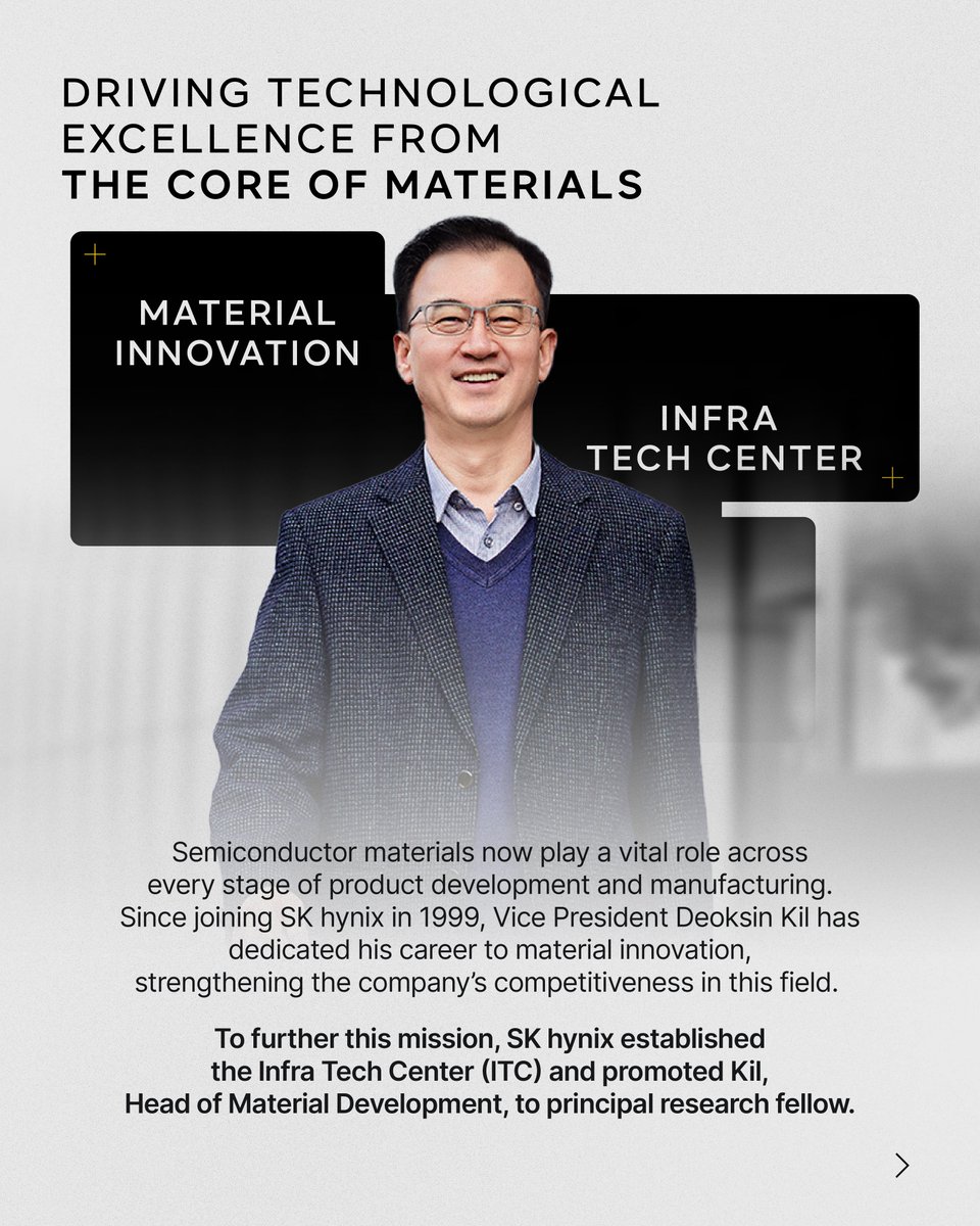
Meet VP Hyunsok Kim, Head of Photo Technology in our 2026 lineup. As the scaling master key, his team stabilized the #EUV process for next-gen #1cDRAM and #HBM to secure extreme yield and quality. #SKhynix #AIMemoryCreator #AI #Leadership
💥 #China’s reported #EUV prototype isn’t the only surprise. U.S. think tank says the country is also pushing older DUVi tools to produce chips nearing leading-edge performance.💡More: buff.ly/HnCe6Os 🔗
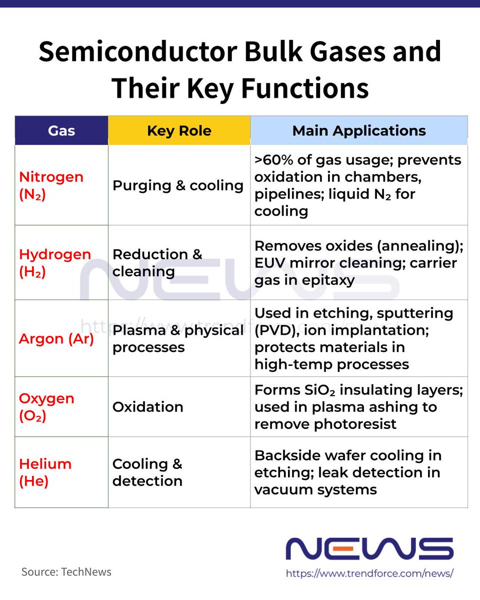
👀 Korea reportedly sources 64.7% of its #helium from #Qatar—but it is just one part of the mix. Iran–U.S. tensions are putting critical chipmaking gases in the spotlight, with applications ranging from #EUV to backside cooling.💡More: pse.is/8velxm 🔗
💰 While #SKhynix eyes a U.S. ADR to fuel its AI memory ambitions, it’s not waiting around—locking in an $8B #EUV deal with #ASML to fast-track its 1c node transition and capacity ramp.💡More: pse.is/8v7p88 🔗

🔎 #TSMC signals A13 will skip High-NA #EUV in 2029. Once holding a reported 56% share of global EUV installations, how will the foundry giant’s strategy reshape #ASML’s long-term outlook? 💡More: pse.is/8zslyk 🔗


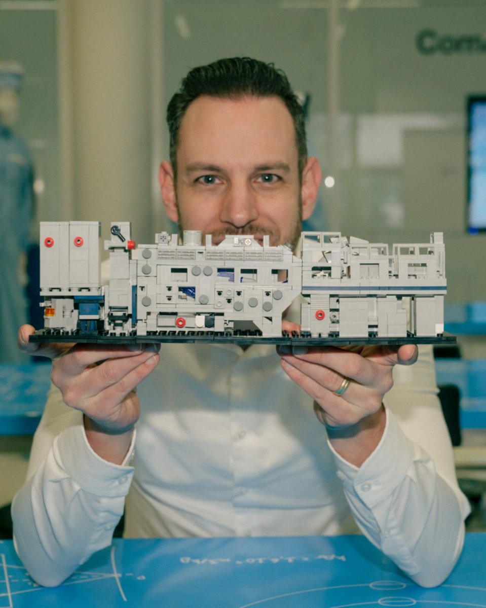
#ASML’s #EUV #Lithography tool has a #LEGO version so coveted that it’s even harder to obtain than the real machine built by its engineers. #Semiconductor #Rapidus

The global race for advanced #AI capabilities runs through a single point of control. A factory in the #Netherlands, called ASML produces the only #EUV machines capable of manufacturing AI chips at scale, with #Washington holding control over access. Middle powers face a choice


ASML je jediným výrobcem na světě, který sériově produkuje stroje pro výrobu čipů pomocí EUV litografie. Letos chce značně navýšit výrobu. #asml #euv #litografie 👉 svethardware.cz/article/asml-c…


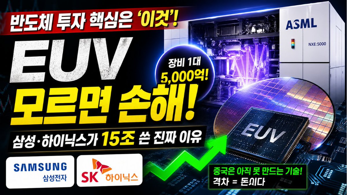
반도체 투자, 딱 하나만 보면 됩니다. EUV. 삼성전자 10조 SK하이닉스 5조 이유는 하나입니다. 👉 이거 없으면 미래 없음 중국도 못 만든 기술 지금 당신은 알고 있나요? #EUV #반도체 #삼성전자 #SK하이닉스 #주식투자
#ASML holds the #EUV chokepoint, but #TSMC’s delay of $400M High-NA tools until 2029 creates a standoff. With #SKHynix moving faster for #AI memory, the monopolist’s "pricing restraint" is under fire. #Semiconductors #TechWar asiatimes.com/2026/04/asml-a…


Litografi Cihazları Üreticisi ASML'den Dev Yatırım yandoki.com/litografi-devi… #euv #semiconductor


💥 中東情勢の混乱がチップ業界に波及 — 日本の材料サプライヤーが #Samsung と #SKhynix に対してリスクを警告したと報じられています。中東産ナフサへの依存度が40%を超えているため、#EUV 用 #フォトレジスト や #HBM


Driven by aggressive capacity adds from HBM vendors (SK Hynix, Samsung, Micron) for HBM3E, HBM4, and HBM4E. EUV remains 66% of ASML revenue. South Korea leads regional demand at 45%. #MemoryChips #EUV
The world's most complex machine - By betting on extreme ultraviolet #lithography long before it worked, #ASML became the chokepoint for cutting-edge chips. worksinprogress.co/issue/the-worl… #EUV #EUVL

🚀 新しい #TSMC ロードマップの発表です! ファウンドリ大手のTSMCは、共に2029年をターゲットとする A12 (1.2nm) および A13 (1.3nm) を公開しました。注目すべきは、いずれもASMLの高NA(High-NA) #EUV 露光装置を必要としない見込みである点です。これは #Intel

🚀 New #TSMC roadmap alert! The foundry giant unveiled A12 (1.2nm) and A13 (1.3nm), both targeting 2029 — and notably, neither is expected to require ASML’s High-NA #EUV. A pointed contrast to #Intel's 14A strategy. 💡More: pse.is/8yuzfd 🔗

Cỗ máy quyền lực nhất ngành chip, định hình cuộc đua AI nghìn tỉ USD 1thegioi.vn/co-may-quyen-l… #asml #euv @ASMLcompany

#China #DUV #EUV #Huawei #DeepSeek #Chips #AI DeepSeek V4 is incredible, but most forget the key: Engrams 🧠 A paradigm shift: separating memory from reasoning. Thanks to them, V4 has 1M context, better reasoning & speed.🔥


UPDATE 🎴 ⚡ $TSM optimalkan mesin EUV lama, delay high-NA $400M sampai 2029! Margin naik tapi risiko bottleneck. ASML aman karena monopoly + demand dari Intel & Samsung. Tapi Wall Street bakal revisi forecast! 📉 #EUV #Semiconductors #TechStocks #Updates Source: Seeking Alpha
💥 Middle East disruptions ripple across chips—Japan’s material suppliers reportedly flag risks to #Samsung and #SKhynix, as >40% reliance on Middle East naphtha may put #EUV #photoresist and #HBM production at risk. 💡More: buff.ly/hGIJkaM 🔗
The global race for advanced #AI capabilities runs through a single point of control. A factory in the #Netherlands, called ASML produces the only #EUV machines capable of manufacturing AI chips at scale, with #Washington holding control over access. Middle powers face a choice


China Invests €37 Billion to Develop Domestic #EUV #Lithography Systems #semiconductor #manufacturing powerelectronicsnews.com/china-invests-…
🚀 New #TSMC roadmap alert! The foundry giant unveiled A12 (1.2nm) and A13 (1.3nm), both targeting 2029 — and notably, neither is expected to require ASML’s High-NA #EUV. A pointed contrast to #Intel's 14A strategy. 💡More: pse.is/8yuzfd 🔗
👀 #ASML’s China revenue held firm in Q1, making up 27% of total sales—while sales in the U.S. and Japan took a hit! 💡Curious about China’s demand and what ASML’s CEO had to say on Chinese #EUV progress? Dive in: buff.ly/lXdVIu0 🔗

IBM and Lam Research expand partnership to develop High-NA #EUV processes aimed at enabling sub-1-nm chips for future #AI systems. eetimes.com/ibm-lam-resear…
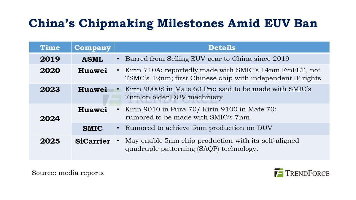
🤔 #ASML’s CEO once believed U.S. #EUV bans would set China’s chip industry back 10–15 years. But is that still the case? Huawei-linked SiCarrier is now eyeing 5nm production using self-aligned quadruple patterning tech!💡More: buff.ly/DyJXmoX 🔗
❗China has secretly built a prototype of a cutting-edge chip-making machine (#EUV lithography) in Shenzhen. It was built by former engineers at the Dutch company ASML. The machine is already producing the special light it needs, but it can’t yet make working chips, per @Reuters.
👀 Korea reportedly sources 64.7% of its #helium from #Qatar—but it is just one part of the mix. Iran–U.S. tensions are putting critical chipmaking gases in the spotlight, with applications ranging from #EUV to backside cooling.💡More: pse.is/8velxm 🔗
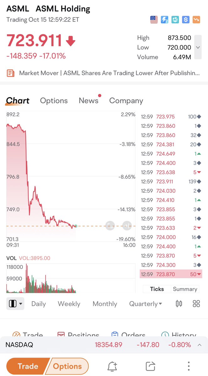
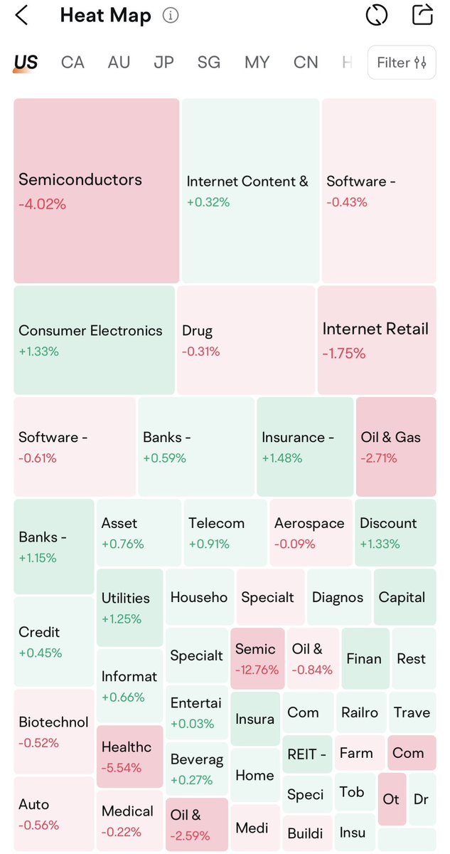
$ASML is down 17% at the moment. Due to a technical error, ASML’s earnings were mistakenly released earlier today, one day ahead of schedule. The entire semiconductor sector is down 4%, likely impacted by the unexpected release. $ASML #EUV #TwinScan #DUV #3nm #AMD $TSM #moomoo
Via #OPG_Optica: Noncollinear, inelastic four-wave mixing in the extreme ultraviolet ow.ly/YFkt50Q5BBJ #EUV #NonlinearOptics @elettrasincro

SemiEngineering's latest Manufacturing, Packaging and Materials Newsletter semiengineering.com/newsletter/mpm… #semiconductor #semiconductormanufacturing #EUV #CMP #ruthenium #GPU #advancedpackaging #DRAM

Key Technologies To Extend EUV To 14 Angstroms Alongside high-NA EUV will be better-performing photoresists, reduced roughness using passivation and etch, and lateral etching to reduce tip-to-tip dimensions. semiengineering.com/key-technologi… #semiconductor #resists #EUV #lithography


Congratulations to @IEEEorg Fellow Tony Yen on his new role as @LifeAtPurdue Distinguished Adjunct Professor! His leadership in #EUV #lithography innovation earned him the 2026 #IEEE Cledo Brunetti Award, sponsored by the Brunetti Bequest: bit.ly/3VfjvH5 #IEEEAwards2026


🚨 j $ASML Q3 Raporu: Beklentileri karışık karşıladı! chip devi #EUV siparişleriyle dikkat çekiyor. 🔷️Net Kâr/Hisse (EPS): 5,48 € (Beklentiyi aştı) ✅ 🔷️Gelir: 7,52 Milyar € (Beklentinin altında) ❌ 🔷️Net Siparişler: 5,4 Milyar € (3,6 Milyar €'su #EUV) 🤩 🤔Gelecek
Currently, #ASML’s revenue contribution from #EUV and #DUV isn’t that far apart. While EUV systems are primarily ordered by #TSMC, #Intel, and #Samsung, the urgency for High NA EUV isn’t quite there yet. Intel and Samsung’s 2nm mass production remains delayed, and even CC admits

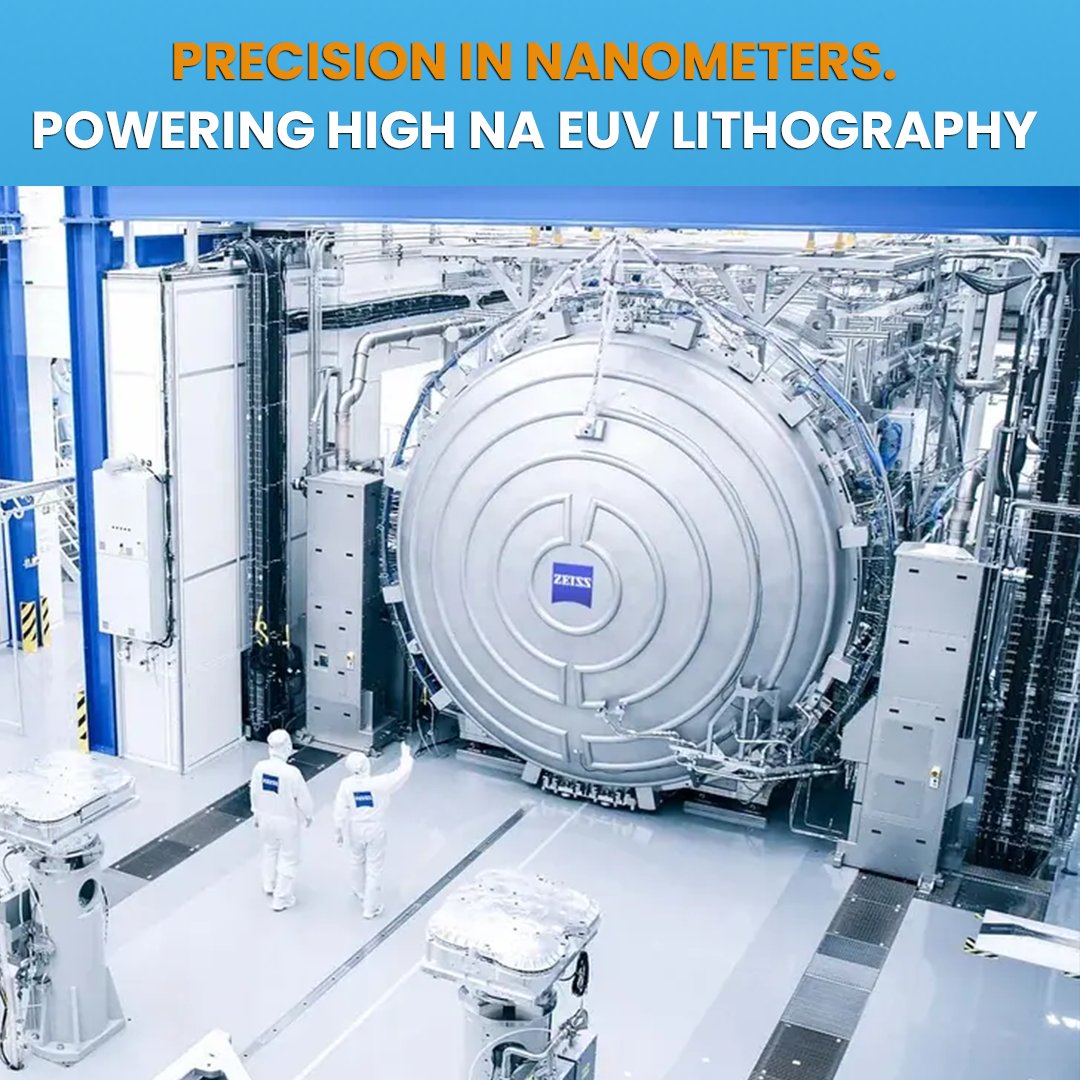
Inside our 5-meter vacuum chambers, we measure ZEISS mirrors in nanometers, driving advancements in High NA EUV lithography. #EUV #Nanotech 📸: Reddit - u/Khornatejester
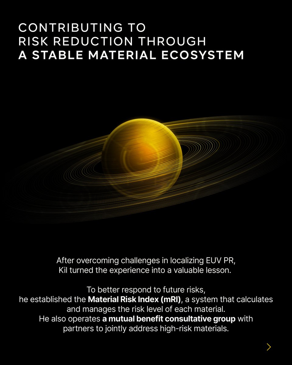
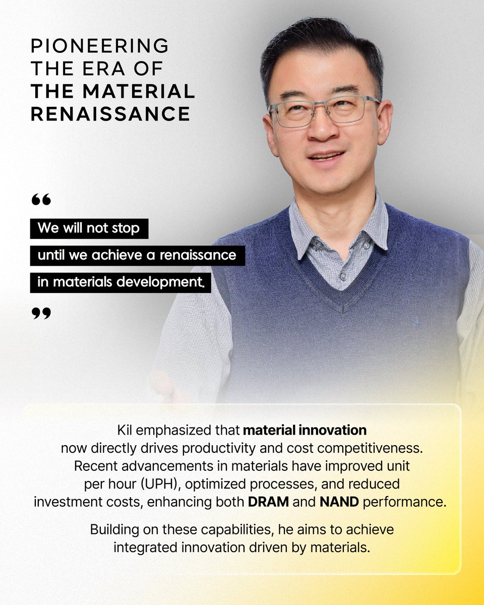
Meet Deoksin Kil, Head of Material Development at #SKhynix. He led the localization of #EUV photoresist, boosting material supply stability, and now drives a “Material Renaissance” through the new Infra Tech Center (#ITC) —advancing semiconductor innovation and performance.


🤯⚙️ Huawei vise le « 2 nm sans EUV » : un brevet qui pourrait rebattre les cartes du semi-conducteur ! Le futur de la fabrication de puces est en pleine mutation. 🔥👇 blog-nouvelles-technologies.fr/350977/huawei-… #Huawei #2nm #EUV #SemiConducteur #Tech #Nouveauté

🤯🔬 La Chine franchit un cap en lithographie avec la machine e-beam Xizhi et les tests d’EUV par Huawei ! Un pas de géant vers l'indépendance technologique. 🔥👇 blog-nouvelles-technologies.fr/337293/chine-x… #Chine #Lithographie #EUV #Huawei #Tech #Innovation #Futur

🤯 Samsung met la main sur une machine High-NA EUV d'ASML ! Un investissement majeur qui pourrait révolutionner la gravure des puces, notamment l'Exynos 2600 ! 🔥 Le futur est en marche 👇 blog-nouvelles-technologies.fr/322460/samsung… 🚀 #Samsung #ASML #EUV #Exynos2600

Something went wrong.
Something went wrong.
United States Trends
- 1. Good Sunday N/A
- 2. #DMDLAND3DAY2 N/A
- 3. Muhammad Qasim N/A
- 4. Sunday Funday N/A
- 5. #SeductiveSunday N/A
- 6. Blessed Sunday N/A
- 7. #SundayVibes N/A
- 8. #SundayReset N/A
- 9. T'Challa N/A
- 10. ZNN LAND OF FUSION D2 N/A
- 11. DMD LAND FINAL ROUND N/A
- 12. KNP DMDD2 THEFINAL N/A
- 13. Bivol N/A
- 14. Championship Sunday N/A
- 15. #SundayMotivation N/A
- 16. Peter Obi N/A
- 17. Shuri N/A
- 18. Black Panther N/A
- 19. Isak N/A
- 20. Old Trafford N/A