#foveros search results

$ONTO metrology will be used by Intel $INTC in #Foveros advanced packaging! Huge upside! They will be ramping from basically 0 volume on this technology to using it for most of their client and datacenter within a few years with Meteor Lake (client) / Granite Rapids (DC)
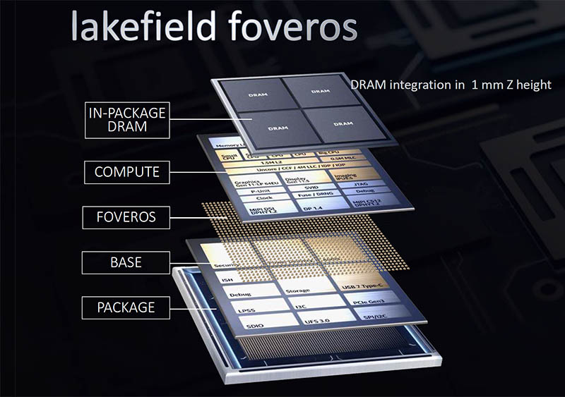
Nice article by @david_schor with some more details on #Lakefield – the base and compute die, the #Foveros Die Interface (FDI). Interesting move by Intel not supporting HT on the Sunny Cove core and disabling AVX (in any way?) to maintain full ISA compatibility across all cores.

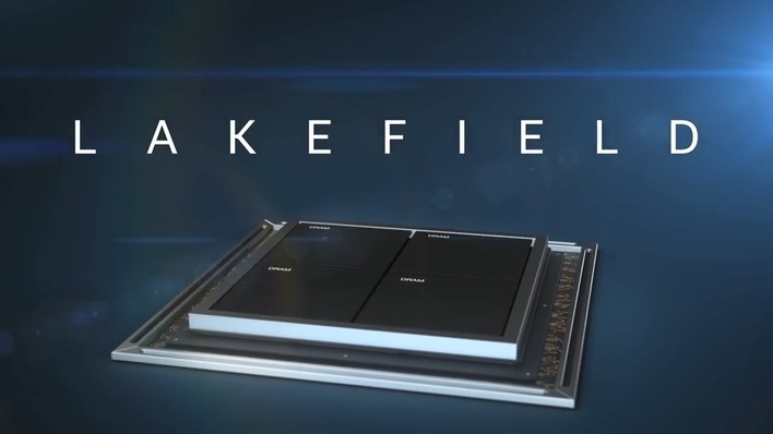
A look at Lakefield: Intel's new mobile-class heterogeneous penta-core SoC. Built using two dies 3D-stacked using Intel's Foveros packaging technology and integrating close to 5 billion transistors, here are the full details: #10nm #22nm #3DIC #x86 fuse.wikichip.org/news/3417/a-lo…
When combined with our world-class process technologies, new packaging capabilities will unlock customer innovations and deliver the computing systems of tomorrow. #Foveros intel.ly/2JpolwY

IFS execs expect to provide Intel’s proprietary EMIB and #Foveros, an advanced 3D face-to-face die-stacking packaging tech, to a “new wave” of customer. eetimes.com/ifs-head-sees-…

By stacking high-performance logic chips for the first time, Intel #Foveros technology opens a world of possibilities for smaller, more efficient, more powerful devices. intel.ly/2FNgR6E

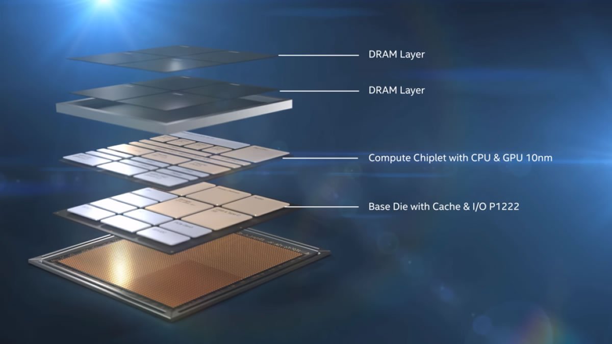
Intel Lakefield Hybrid SoC detailed. 10nm 3D Foveros with compute, an I/O die, and in-package DRAM. This even brings large Sunny Cove and small Tremont cores to a single SoC. Chiplets are the future. servethehome.com/intel-lakefiel… @IntelBusiness #Foveros
The silicon nerd in me is going crazy seeing this. Those packages are huge and I can’t wait until we see Co-EMIB in actual chips. ODI seems to give Intel more flexibility on the physical design and how to arrange the different layers. #EMIB #FOVEROS #ODI #MDIO

.@Intel announced three new chip technologies that should find their way into future chips here at #SemiconWest19 including ODI (omnidirectional interconnect), Co-EMIB (Foveros+EMIB), and MDIO (Multi-Die IO) that leverages Intel's AIB (Advanced Interface Bus) PHY interconnect.


Intel's announcement of #Foveros helps the company to navigate the competitive landscape more effectively and gives them an opportunity to innovate in different places at different speeds. Im excited to see this productized and how it'll stack up to the competition (pun intended)

Great interview with @RamuneTunes of @intel, discussing packaging technologies, the future research of tech like #Foveros, Intel's chiplet strategy, enabling a chiplet ecosystem, and the direct importance of DTCO in an optimised product portfolio. Transcription soon. #IEDM2019
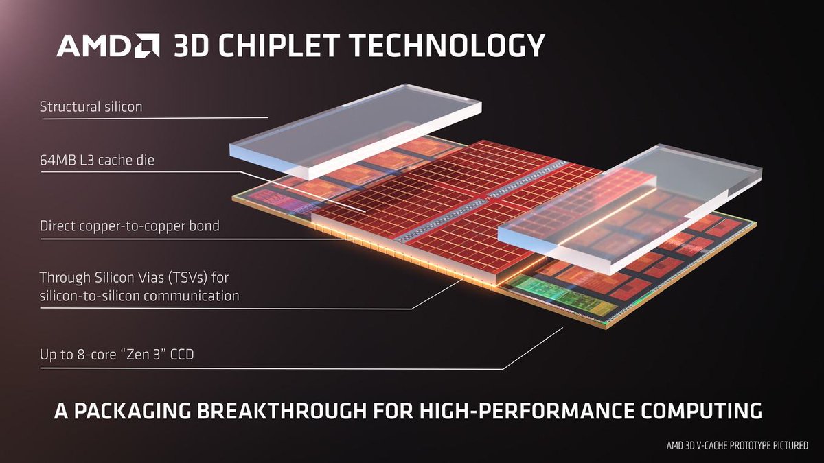
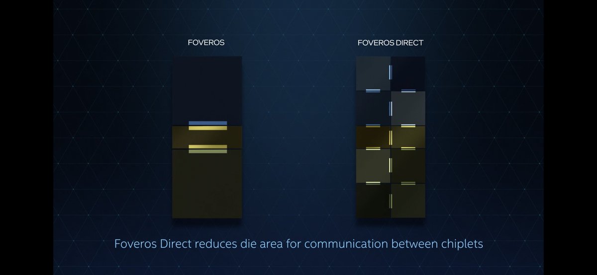
With #Foveros Direct Intel talks about stacking cache on top of a compute tile. Did they say AMD 3D V-Cache?


#TodaysTips🗒️ 🏇Wexford➡️1st race➡️12.50pm 🏇Galway➡️1st race➡️1.05pm Jumps action at both @WexfordRacecour and @Galway_Races this afternoon. Don't get caught out by the earlier start times! Our preview of both meetings is here👇#Foveros bit.ly/2JxUTpW


#IntelLakefield: así es el primer procesador de cinco núcleos y tecnología #Foveros ----> culturageek.com.ar/intel-lakefiel…
The silicon marvel of packaging: Intel #Lakefield. In some ways, the processor was ahead of its time, but the technology was also simply wrongly positioned as a product. I talked with some of the #Foveros Engineers last year, they were full of pride for what they have achieved.


#Intel #Lakefield CPU WIth Revolutionary #Foveros 3D Tech Previewed - 10nm Sunny Cove, Gen 11 Graphics, PoP DRAM wccftech.com/intel-lakefiel…

It's time to rethink how we create computer #processors, says @jckgld – and @Intel is leading the way with #Foveros ow.ly/DAfz30n1n9A #MooresLaw
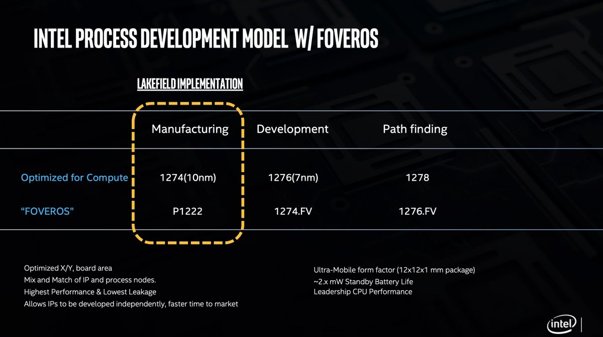
On future Lakefield generations: For the next generation, Intel wants to manufacture the base die in 10 nm #Foveros (P1274.FV). The compute die is supposed to change to 7 nm (P1276). The generation after next is 7 nm (P1276.FV) for the base and 5 nm (P1278) for the compute die.

#IntelLakefield: así es el primer procesador de cinco núcleos y tecnología #Foveros ----> culturageek.com.ar/intel-lakefiel…


🔧 Intel EMIB y Foveros ganan interés en la industria ⚙️ Apple y Qualcomm buscan ingenieros con estas tecnologías 🚀 Alternativa al saturado CoWoS de TSMC 📌 Oportunidad para Intel Foundry Services #Intel #EMIB #Foveros #TSMC #FanáticosDelHardware fanaticosdelhardware.com/intel-atrae-in…


②新しい冷却素材と構造 注目「熱を逃がす構造」 ✅ ダイヤモンド薄膜:熱伝導率は銅の5倍 ✅ 液冷プレート:冷媒を直接チップ裏に流す ✅ マイクロチャネル:3D-ICの層間を冷却 これらは単なる冷却装置ではなく “回路設計の一部”として最適化される時代へ #CoWoS #Foveros #ダイヤモンド #液冷 ↓

Nvidia invests $5 billion in Intel's advanced chip packaging tech, like Foveros, to boost AI chip performance and diversify its supply chain. #Nvidia #Intel #Foveros turtnws.biz.id/2025/09/how-in…
turtnws.biz.id
How Intel's Packaging Technology Became the Cornerstone of Nvidia's $5 Billion Bet
How Intel's Packaging Technology Became the Cornerstone of Nvidia's $5 Billion Bet

Major tech companies seeking alternatives are turning to Intel’s IFS. Since Intel’s #Foveros is said to be comparable to TSMC’s CoWoS-S, it has made Intel’s #advancedpackaging a viable option to ensure supply. $MSFT Confirmed Potential customers $NVDA $CSCO #semiconductor

The silicon marvel of packaging: Intel #Lakefield. In some ways, the processor was ahead of its time, but the technology was also simply wrongly positioned as a product. I talked with some of the #Foveros Engineers last year, they were full of pride for what they have achieved.

14:15 #Catterick #BaronDeMidleton or #Foveros Who's your pick? All prices available here: starspreads.com/events/daily-i…
IFS execs expect to provide Intel’s proprietary EMIB and #Foveros, an advanced 3D face-to-face die-stacking packaging tech, to a “new wave” of customer. eetimes.com/ifs-head-sees-…

Intel Clearwater Forest Xeon CPUs With Up To 288 E-Cores To Utilize Foveros Direct 3D Stacking Technology #Wccftech #Intel #Foveros wccftech.com/intel-clearwat…
wccftech.com
Intel Clearwater Forest Xeon CPUs With Up To 288 E-Cores To Utilize Foveros Direct 3D Stacking...
Intel Clearwater Forest Xeon CPUs will be making use of Foveros Direct technology to 3D Stack up to 288 cores on top of the base tile.


Intel Lakefield Hybrid SoC detailed. 10nm 3D Foveros with compute, an I/O die, and in-package DRAM. This even brings large Sunny Cove and small Tremont cores to a single SoC. Chiplets are the future. servethehome.com/intel-lakefiel… @IntelBusiness #Foveros

「 #FOVERÓS 1st Open Member 」 Classic squad for elegant boys and girls. 🗓️ : Friday, 17 April 2O2O 🏘 : @FOVEROSQ Timeline's 🕗 : NOW Let's come and join us ! ! !
IFS execs expect to provide Intel’s proprietary EMIB and #Foveros, an advanced 3D face-to-face die-stacking packaging tech, to a “new wave” of customer. eetimes.com/ifs-head-sees-…
Great interview with @RamuneTunes of @intel, discussing packaging technologies, the future research of tech like #Foveros, Intel's chiplet strategy, enabling a chiplet ecosystem, and the direct importance of DTCO in an optimised product portfolio. Transcription soon. #IEDM2019
Bis zu 36 Chips auf einem Package - #EMIB und #FOVEROS als Co-EMIB vereint. Hinzu kommen #ODI und #MDIO. @Intel_DE richtet sich vollständig auf die #Chiplet-Zukunft aus: hardwareluxx.de/index.php/news…
The silicon marvel of packaging: Intel #Lakefield. In some ways, the processor was ahead of its time, but the technology was also simply wrongly positioned as a product. I talked with some of the #Foveros Engineers last year, they were full of pride for what they have achieved.
With #Foveros Direct Intel talks about stacking cache on top of a compute tile. Did they say AMD 3D V-Cache?


On future Lakefield generations: For the next generation, Intel wants to manufacture the base die in 10 nm #Foveros (P1274.FV). The compute die is supposed to change to 7 nm (P1276). The generation after next is 7 nm (P1276.FV) for the base and 5 nm (P1278) for the compute die.
#IntelLakefield: así es el primer procesador de cinco núcleos y tecnología #Foveros ----> culturageek.com.ar/intel-lakefiel…
#Intel nous reparle de son #SoC Multicouches #Foveros #Lakefield et le compare à un gros gâteau dlvr.it/RPxVcW

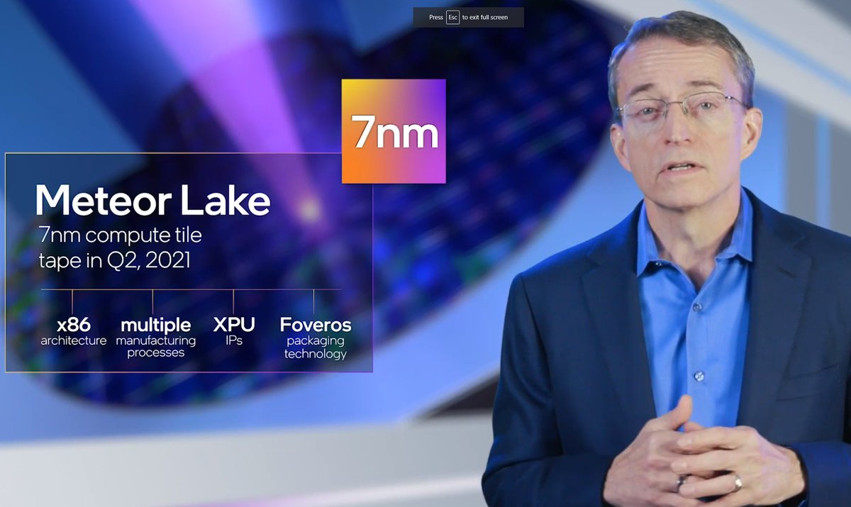
.@Intel Meteor Lake is based on 7nm and will be taped in Q2 2021 using #Foveros packaging technology! He also showed off Ponte Vecchio! #Intel

In einem Video erläutert @Intel_DE den Aufbau von #Foveros und des #Lakefield-SoC: hardwareluxx.de/index.php/news…


#Intel introduced #3D packing technology, #Foveros, which allows for stacking of more #transistors and other components into #chips, helping industry to continue #MooresLaw. Consumer products using Foveros are expected to launch in #2019 bit.ly/2CkNFzI

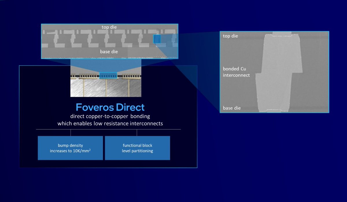
Intel already talked about #Foveros Direct HBI at the Accelerated event. The challenge here is the correct alignment of the dies, which are then connected to each other via the bonded Cu interconnect. It requires several test stages to be executed correctly.

#IntelLakefield: así es el primer procesador de cinco núcleos y tecnología #Foveros ----> culturageek.com.ar/intel-lakefiel…
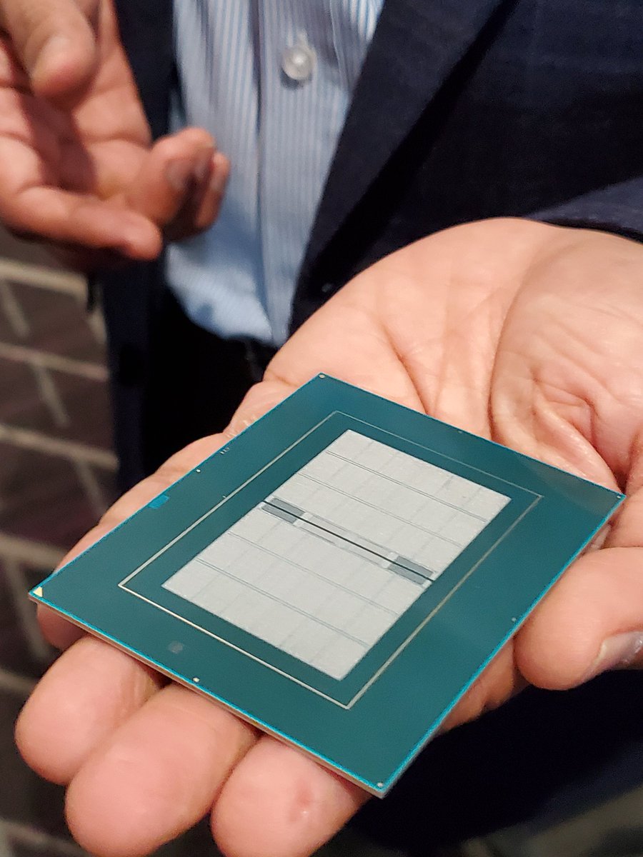
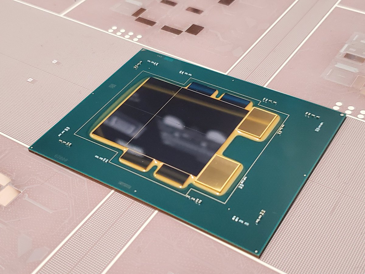
A test package of #MeteorLake with #Foveros wafer level assembly. It’s a test package, because it would probably not be economically feasible that way.

Something went wrong.
Something went wrong.
United States Trends
- 1. Luka N/A
- 2. #LakeShow N/A
- 3. Miami Ohio N/A
- 4. Rockets N/A
- 5. #Survivor50 N/A
- 6. Qatar N/A
- 7. #TexasHockey N/A
- 8. Nico Harrison N/A
- 9. #Lakers N/A
- 10. #AEWDynamite N/A
- 11. THE 25TH PERTH CHAPTER N/A
- 12. Sengun N/A
- 13. Redhawks N/A
- 14. Toluca N/A
- 15. Zac Brown N/A
- 16. Tari Eason N/A
- 17. Otter N/A
- 18. WEVERSE IN OUR ZONE N/A
- 19. Jake Oettinger N/A
- 20. Jabari N/A