#highdensitypcb search results

IC Substrate PCB series: HDI (High Density Interconnect), CPU-package, SIM (mobile communication), Mini LED, Electronic, EMMC (Embedded Multimedia Card) and BGA (Ball Grid Array) #ICSubstratePCB #HighDensityPCB #TelecommunicationPCB #DataStoragePCB #MiniLEDPCB #ElectronicPCB


Tips you will need to design a successful HDI PCB buff.ly/2gmSdw3 #HighDensityInterconnect #HighDensityPCB #circuitboard


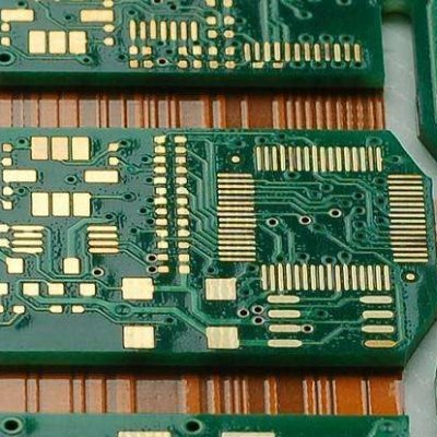
An HDI PCB is defined as a printed circuit board with a higher wiring density per unit area than a conventional PCB. Contact me at [email protected] or view hitechcircuits.com/high-density-i… #HDIpcb #HighDensityPCB

High Density Interconnect PCB, HDI PCB Manufacturing HDI board China High Density Interconnects (HDI PCB) Board are used to meet the market demand for complex designs in smaller form factors... #HighDensityPCB #HDIPCB hitechcircuits.com/high-density-i…


Designers must consider processing temperatures, producibility, and solder joint integrity of every component as well as higher I/O connectors. Find out how to enable smaller component footprints for high-density: bit.ly/3nduhKE #PCBs #highdensityPCB


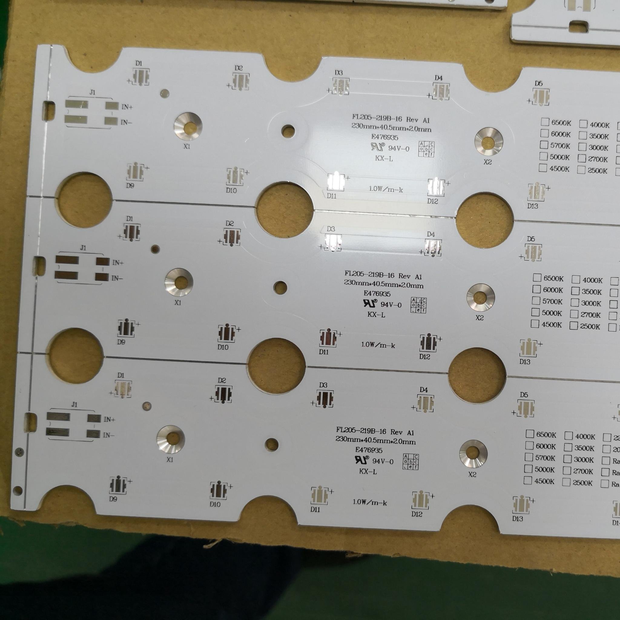
HOYOGO produce #HighDensityPCB. Here is 6 layer high density #PCB. #FR4 #HASLLeadFree Min Hole Size: 0.25mm #PCBA #PCBdesign #HoYoGoPCBManufacturer Find me at: Email: [email protected] Skype: live:sales21_205 Website: hoyogo.com

HOYOGO #HighDensityPCB The picture below is our high quality 6 layer #FR4 #TG170 rigid PCB. hoyogo.com Special Request: #BlindBuriedVia Final Copper Thickness: #1OZ Surface Finished: #ENIG+ #ImpedanceControl Min Hole Size: 0.15mm #pcb #circuitboard #pcbfactory

High-Density PCB: Impact on the Industry and Continuous Exploration capelfpc.com/news/high-dens… #HighDensityPCB #FlexiblePCB #RigidFlexiblePCB #HDIPCB #PCBDesign #CircuitBoard #Electronicproducts #Technology #Innovation #InternetofThings

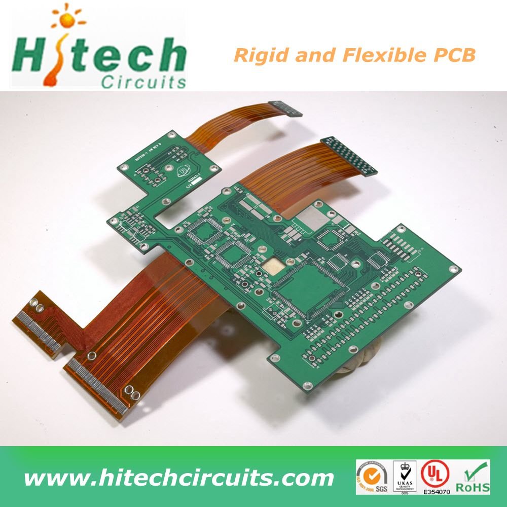
we can provide from 1 to 38 layers of PCB products, which includes double layers PCB, Multilayer PCB, Metal core PCB, Rigid-Flex PCB and High Density (HDI) PCB, PCB assembly service, etc. #Regidpcb #multilayer #HighDensityPCB hitechcircuits.com/high-quality-r…


linkedin.com/posts/activity… Learn About HDI Printed Circuit Board #hdipcb #highdensitypcb efpcb.com/pcb-blog/ems-i…

Using the HDI Stackup Planner before you begin your layout design will ensure that your HDI PCB design will be manufacturable the very first time. youtube.com/watch?v=RuBAs-… #hdi #hdipcb #highdensitypcb #highdensityboard #pcbmanufacturer #pcbdesign
HDI pcb is the abbreviation for High Density Interconnect pcb or High Density pcb. An HDI PCB is defined as a printed circuit board with a higher wiring density per unit area than a conventional PCB. #HDIPCB #HighDensityPCB hitechcircuits.com/high-density-i…
#PCB #SMT #PCBA #Components #HDI The FQC station in our factory, please have a look. All single board will be check carefully before shipping. If you have any pcb or pcb assembly project, just contact us directly. Read more: hitechcircuits.com Email us: [email protected]
High-Density PCB: Impact on the Industry and Continuous Exploration capelfpc.com/news/high-dens… #HighDensityPCB #FlexiblePCB #RigidFlexiblePCB #HDIPCB #PCBDesign #CircuitBoard #Electronicproducts #Technology #Innovation #InternetofThings
linkedin.com/posts/activity… Learn About HDI Printed Circuit Board #hdipcb #highdensitypcb efpcb.com/pcb-blog/ems-i…
Using the HDI Stackup Planner before you begin your layout design will ensure that your HDI PCB design will be manufacturable the very first time. youtube.com/watch?v=RuBAs-… #hdi #hdipcb #highdensitypcb #highdensityboard #pcbmanufacturer #pcbdesign
Designers must consider processing temperatures, producibility, and solder joint integrity of every component as well as higher I/O connectors. Find out how to enable smaller component footprints for high-density: bit.ly/3nduhKE #PCBs #highdensityPCB

An HDI PCB is defined as a printed circuit board with a higher wiring density per unit area than a conventional PCB. contact me at [email protected] View more : pcba123.com #HDIpcb #HighDensityPCB

An HDI PCB is defined as a printed circuit board with a higher wiring density per unit area than a conventional PCB. Contact me at [email protected] or view hitechcircuits.com/high-density-i… #HDIpcb #HighDensityPCB
we can provide from 1 to 38 layers of PCB products, which includes double layers PCB, Multilayer PCB, Metal core PCB, Rigid-Flex PCB and High Density (HDI) PCB, PCB assembly service, etc. #Regidpcb #multilayer #HighDensityPCB hitechcircuits.com/high-quality-r…
HDI pcb is the abbreviation for High Density Interconnect pcb or High Density pcb. An HDI PCB is defined as a printed circuit board with a higher wiring density per unit area than a conventional PCB. #HDIPCB #HighDensityPCB hitechcircuits.com/high-density-i…
#PCB #SMT #PCBA #Components #HDI The FQC station in our factory, please have a look. All single board will be check carefully before shipping. If you have any pcb or pcb assembly project, just contact us directly. Read more: hitechcircuits.com Email us: [email protected]
High Density Interconnect PCB, HDI PCB Manufacturing HDI board China High Density Interconnects (HDI PCB) Board are used to meet the market demand for complex designs in smaller form factors... #HighDensityPCB #HDIPCB hitechcircuits.com/high-density-i…
Tips you will need to design a successful HDI PCB buff.ly/2gmSdw3 #HighDensityInterconnect #HighDensityPCB #circuitboard
Tips you will need to design a successful HDI PCB buff.ly/2gmSdw3 #HighDensityInterconnect #HighDensityPCB #circuitboard
IC Substrate PCB series: HDI (High Density Interconnect), CPU-package, SIM (mobile communication), Mini LED, Electronic, EMMC (Embedded Multimedia Card) and BGA (Ball Grid Array) #ICSubstratePCB #HighDensityPCB #TelecommunicationPCB #DataStoragePCB #MiniLEDPCB #ElectronicPCB
High Density Interconnect PCB, HDI PCB Manufacturing HDI board China High Density Interconnects (HDI PCB) Board are used to meet the market demand for complex designs in smaller form factors... #HighDensityPCB #HDIPCB hitechcircuits.com/high-density-i…
Designers must consider processing temperatures, producibility, and solder joint integrity of every component as well as higher I/O connectors. Find out how to enable smaller component footprints for high-density: bit.ly/3nduhKE #PCBs #highdensityPCB
we can provide from 1 to 38 layers of PCB products, which includes double layers PCB, Multilayer PCB, Metal core PCB, Rigid-Flex PCB and High Density (HDI) PCB, PCB assembly service, etc. #Regidpcb #multilayer #HighDensityPCB hitechcircuits.com/high-quality-r…
HOYOGO produce #HighDensityPCB. Here is 6 layer high density #PCB. #FR4 #HASLLeadFree Min Hole Size: 0.25mm #PCBA #PCBdesign #HoYoGoPCBManufacturer Find me at: Email: [email protected] Skype: live:sales21_205 Website: hoyogo.com
An HDI PCB is defined as a printed circuit board with a higher wiring density per unit area than a conventional PCB. Contact me at [email protected] or view hitechcircuits.com/high-density-i… #HDIpcb #HighDensityPCB
HOYOGO #HighDensityPCB The picture below is our high quality 6 layer #FR4 #TG170 rigid PCB. hoyogo.com Special Request: #BlindBuriedVia Final Copper Thickness: #1OZ Surface Finished: #ENIG+ #ImpedanceControl Min Hole Size: 0.15mm #pcb #circuitboard #pcbfactory
High-Density PCB: Impact on the Industry and Continuous Exploration capelfpc.com/news/high-dens… #HighDensityPCB #FlexiblePCB #RigidFlexiblePCB #HDIPCB #PCBDesign #CircuitBoard #Electronicproducts #Technology #Innovation #InternetofThings
Something went wrong.
Something went wrong.
United States Trends
- 1. Veterans Day 81.7K posts
- 2. Good Tuesday 30.3K posts
- 3. Mainz Biomed N/A
- 4. SoftBank 8,249 posts
- 5. United States Armed Forces N/A
- 6. #tuesdayvibe 1,789 posts
- 7. Vets 13.6K posts
- 8. #Talus_Labs N/A
- 9. Armistice Day 11.9K posts
- 10. #Gratitude 1,434 posts
- 11. Bond 61.5K posts
- 12. #ARMY 1,584 posts
- 13. #RemembranceDay 11.8K posts
- 14. World War 39.7K posts
- 15. 600k Chinese 6,027 posts
- 16. $NBIS 6,744 posts
- 17. 600,000 Chinese 10.9K posts
- 18. Window 54K posts
- 19. Islamabad 42.1K posts
- 20. Berkeley 101K posts