#pcbstackup search results

Dan Beeker tells you which basic errors to avoid in your stack-up. Watch his full interview here: youtube.com/watch?v=Yb0wWW… #pcb #circuitboard #pcbstackup #pcbdesign #emi #emc #pcbwest @PCBWest
We have a lot of tools to help #PCBDesigners. Try our Stackup Planner, Impedance Calculator, BOM Checker, and more... #pcbstackup #impedance #controlledimpedance #characteristicimpedance #bom #billofmaterials #pcba #pcbassembly #pcbtool

Coenrichpcb tips for pcb stackup design for pcb layout designer / [email protected] #pcbdesign #pcblayout #pcbstackup #pcbadesign

#PCBStackup #StackupTool Using the Stackup Planner before you begin your layout design will ensure that your PCB design will be manufacturable the very first time. Try it now: protoexpress.com/pcb/hdi-pcb-st…

6 aspects to consider designing ur PCB buff.ly/2b7wZOc #PCBStackup #Via #DesignRule #boarddesign #PCBLayout


Keeping track of characteristic impedance, trace width, ground plane and other #PCBmaterials can make frequency management and a #PCBstackup nearly unmanageable. Thankfully, there is software that can help keep track for you. altium.com/solution/pcb-t…

Using your PCB House's standard circuit board layer stackup to achieve quick fabrication buff.ly/2ymDnA2 #PCBStructure #PCBStackup

Designing a reference plane might seem as simple as laying a ground plane in an interior layer. Combining the right #routing strategy with an appropriate #pcbstackup can help solve some common signal integrity problems in your next multilayer #PCB. bit.ly/2Xf9SIw

Why PCB Manufacturers apply layer stack-up during multi-layer PCB fabrication? buff.ly/2u9wyQb #PCBStackup #PCBCart #CircuitBoards

Kella Knack revisits the history of the #PCBstackup process and shares tips on how to guarantee your product works right the first time while meeting all mechanical and electrical performance criteria. bit.ly/2GC54GQ #rightthefirsttime #electronicsdesign #pcbdesign

How to get better wireless performance for mobile devices with smaller #PCBs bit.ly/3c7RRmU #pcbdesign #PCBstackup #pcblayout #antenna

Try our Signal and Power Layer Estimator tool! protoexpress.com/tools/signal-l… #pcb #pcbdeisgn #pcbstackup #engineering #hardware #circuitboard


Optimize your circuit design with our 4-layer PCB stackups at SFX PCB. Discover how our stackup solutions can improve your project’s performance. bit.ly/4c2uZ6w #4LayerPCB #PCBStackup #SignalRouting #ElectronicsDesign
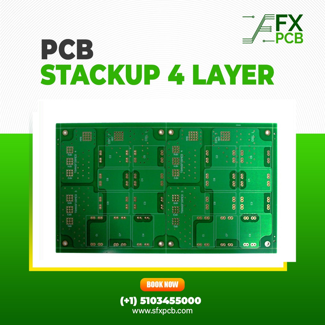
Optimize your designs with S FX PCB's 4-layer PCB stackup. Our advanced technology ensures precise and reliable multilayer boards for your projects. Visit our website to learn more! bit.ly/4c2uZ6w #4LayerPCB #AdvancedDesign #PCBStackup #SFXPCB

A 16-layer stack-up PCB comprises 16 distinct layers of conductive and insulating materials. Click here to read more ow.ly/pGMU50P4Qi6 #PCBDirectory #16LayerPCB #PCBStackup #PCBDesign #PCBLayers #PCBTechnology #PCBMaterials #PCBDirectoryCommunity


PCB STACK-UP? #PCBstackup help you in balancing your need for low-cost, efficient manufacturing methods with concerns about signal integrity issues. ✌👍 👉 It’s an arrangement of #copperlayers. Get more about 4 layer #PCB stack:👇👇 greatpcb.com/pcb-stack-up/ #GREATPCB


Four-layer PCB – The design Rules and how to make Heavy Copper inner H OZ-4 OZ, outter 1 OZ-15 OZ hx-circuit.com/four-layer-pcb… #FourlayerPCB #PCBDesign #PCBStackup #4LayerPCB #HeavyCopperPCB
A 4-layer stack-up PCB refers to a printed circuit board configuration that consists of four distinct layers of conductive and insulating materials. Click here to learn more ow.ly/EzKQ50Rtowb #pcb #technical #pcbstackup #design #signal #article #post #industry #directory

The #Stackup Designer provides precise options for cost-optimized build-up structures and includes an impedance calculator to get the desired impedance and trace and space values on any signal layer. bit.ly/33WIhzY #pcb #pcbstackup #pcbdesign #pcbmanufacturer


Standard 4-Layer PCB Stack-up: Design, Fabrication, and the cost of manufacturing! buff.ly/3y8ymrd #PCBStackup #4LayerPCB #PCBDesign #PCBFabricaton #PCBCost

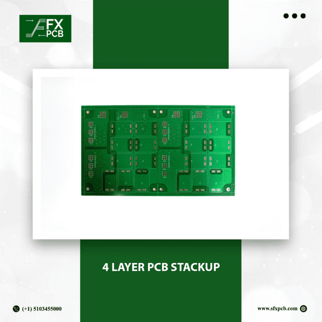
Optimize your circuit design with our 4-layer PCB stackups at SFX PCB. Discover how our stackup solutions can improve your project’s performance. bit.ly/4c2uZ6w #4LayerPCB #PCBStackup #SignalRouting #ElectronicsDesign
Optimize your designs with S FX PCB's 4-layer PCB stackup. Our advanced technology ensures precise and reliable multilayer boards for your projects. Visit our website to learn more! bit.ly/4c2uZ6w #4LayerPCB #AdvancedDesign #PCBStackup #SFXPCB
A 4-layer stack-up PCB refers to a printed circuit board configuration that consists of four distinct layers of conductive and insulating materials. Click here to learn more ow.ly/EzKQ50Rtowb #pcb #technical #pcbstackup #design #signal #article #post #industry #directory
The #Stackup Designer provides precise options for cost-optimized build-up structures and includes an impedance calculator to get the desired impedance and trace and space values on any signal layer. bit.ly/33WIhzY #pcb #pcbstackup #pcbdesign #pcbmanufacturer
A 16-layer stack-up PCB comprises 16 distinct layers of conductive and insulating materials. Click here to read more ow.ly/pGMU50P4Qi6 #PCBDirectory #16LayerPCB #PCBStackup #PCBDesign #PCBLayers #PCBTechnology #PCBMaterials #PCBDirectoryCommunity
Try our Signal and Power Layer Estimator tool! protoexpress.com/tools/signal-l… #pcb #pcbdeisgn #pcbstackup #engineering #hardware #circuitboard

Understanding the standard PCB layer stack-up is crucial for successful PCB design. With the right layer configuration, for optimize your board's performance and ensure reliable operation:bit.ly/3KasHrl #PCBdesign #PCBstackup #PCBlayers #circuitboard #PCBconfiguration
Standard 4-Layer PCB Stack-up: Design, Fabrication, and the cost of manufacturing! buff.ly/3y8ymrd #PCBStackup #4LayerPCB #PCBDesign #PCBFabricaton #PCBCost
Coenrichpcb tips for pcb stackup design for pcb layout designer / [email protected] #pcbdesign #pcblayout #pcbstackup #pcbadesign
Four-layer PCB – The design Rules and how to make Heavy Copper inner H OZ-4 OZ, outter 1 OZ-15 OZ hx-circuit.com/four-layer-pcb… #FourlayerPCB #PCBDesign #PCBStackup #4LayerPCB #HeavyCopperPCB
We have a lot of tools to help #PCBDesigners. Try our Stackup Planner, Impedance Calculator, BOM Checker, and more... #pcbstackup #impedance #controlledimpedance #characteristicimpedance #bom #billofmaterials #pcba #pcbassembly #pcbtool
#PCBStackup #StackupTool Using the Stackup Planner before you begin your layout design will ensure that your PCB design will be manufacturable the very first time. Try it now: protoexpress.com/pcb/hdi-pcb-st…
This tool offers precise options for cost-optimized stack-up structures and has an integrated Impedance Calculator to get desired impedance and trace/space values. bit.ly/33WIhzY #pcbstackup #pcbdesign #pcbdesigner #pcbmanufacturer #pcbfab #ee #hardware

Dan Beeker tells you which basic errors to avoid in your stack-up. Watch his full interview here: youtube.com/watch?v=Yb0wWW… #pcb #circuitboard #pcbstackup #pcbdesign #emi #emc #pcbwest @PCBWest
How to achieve best possible PCB stack-up design. bit.ly/3d0kbID #pcb #circuitboard #pcbstackup #stackup #pcbdesign #pcbmanufacturing
How to get better wireless performance for mobile devices with smaller #PCBs bit.ly/3c7RRmU #pcbdesign #PCBstackup #pcblayout #antenna
6 aspects to consider designing ur PCB buff.ly/2b7wZOc #PCBStackup #Via #DesignRule #boarddesign #PCBLayout
Why PCB Manufacturers apply layer stack-up during multi-layer PCB fabrication? buff.ly/2u9wyQb #PCBStackup #PCBCart #CircuitBoards
How to get better wireless performance for mobile devices with smaller #PCBs bit.ly/3c7RRmU #pcbdesign #PCBstackup #pcblayout #antenna
Using your PCB House's standard circuit board layer stackup to achieve quick fabrication buff.ly/2ymDnA2 #PCBStructure #PCBStackup
Coenrichpcb tips for pcb stackup design for pcb layout designer / [email protected] #pcbdesign #pcblayout #pcbstackup #pcbadesign
Try our Signal and Power Layer Estimator tool! protoexpress.com/tools/signal-l… #pcb #pcbdeisgn #pcbstackup #engineering #hardware #circuitboard
Keeping track of characteristic impedance, trace width, ground plane and other #PCBmaterials can make frequency management and a #PCBstackup nearly unmanageable. Thankfully, there is software that can help keep track for you. altium.com/solution/pcb-t…
Designing a reference plane might seem as simple as laying a ground plane in an interior layer. Combining the right #routing strategy with an appropriate #pcbstackup can help solve some common signal integrity problems in your next multilayer #PCB. bit.ly/2Xf9SIw
Kella Knack revisits the history of the #PCBstackup process and shares tips on how to guarantee your product works right the first time while meeting all mechanical and electrical performance criteria. bit.ly/2GC54GQ #rightthefirsttime #electronicsdesign #pcbdesign
A 16-layer stack-up PCB comprises 16 distinct layers of conductive and insulating materials. Click here to read more ow.ly/pGMU50P4Qi6 #PCBDirectory #16LayerPCB #PCBStackup #PCBDesign #PCBLayers #PCBTechnology #PCBMaterials #PCBDirectoryCommunity
A 4-layer stack-up PCB refers to a printed circuit board configuration that consists of four distinct layers of conductive and insulating materials. Click here to learn more ow.ly/EzKQ50Rtowb #pcb #technical #pcbstackup #design #signal #article #post #industry #directory
The #Stackup Designer provides precise options for cost-optimized build-up structures and includes an impedance calculator to get the desired impedance and trace and space values on any signal layer. bit.ly/33WIhzY #pcb #pcbstackup #pcbdesign #pcbmanufacturer
Standard 4-Layer PCB Stack-up: Design, Fabrication, and the cost of manufacturing! buff.ly/3y8ymrd #PCBStackup #4LayerPCB #PCBDesign #PCBFabricaton #PCBCost
PCB STACK-UP? #PCBstackup help you in balancing your need for low-cost, efficient manufacturing methods with concerns about signal integrity issues. ✌👍 👉 It’s an arrangement of #copperlayers. Get more about 4 layer #PCB stack:👇👇 greatpcb.com/pcb-stack-up/ #GREATPCB
Optimize your circuit design with our 4-layer PCB stackups at SFX PCB. Discover how our stackup solutions can improve your project’s performance. bit.ly/4c2uZ6w #4LayerPCB #PCBStackup #SignalRouting #ElectronicsDesign
Optimize your designs with S FX PCB's 4-layer PCB stackup. Our advanced technology ensures precise and reliable multilayer boards for your projects. Visit our website to learn more! bit.ly/4c2uZ6w #4LayerPCB #AdvancedDesign #PCBStackup #SFXPCB
Something went wrong.
Something went wrong.
United States Trends
- 1. Epstein 1.22M posts
- 2. #AEWDynamite 13.8K posts
- 3. #AEWBloodAndGuts 2,202 posts
- 4. Skye Blue 1,784 posts
- 5. Cy Young 15.1K posts
- 6. Paul Skenes 10.4K posts
- 7. Tarik Skubal 6,475 posts
- 8. Raising Arizona N/A
- 9. Blood & Guts 11.7K posts
- 10. Virginia Giuffre 68.7K posts
- 11. Starship 14.9K posts
- 12. Steam Machine 65.3K posts
- 13. Igor 8,941 posts
- 14. Bill Clinton 29.7K posts
- 15. #ChicagoMed N/A
- 16. Valve 44.1K posts
- 17. #GoBolts N/A
- 18. Blanca 26.2K posts
- 19. #dispatch 62.6K posts
- 20. Borgen N/A