#siliconphotonics search results
#InnovativeTsinghua researchers proposed a reconfigurable #quantum entanglement distribution network using #siliconphotonics, reducing wavelength channels to O(N) and improving the scalability, reconfigurability, and performance of quantum technology. bit.ly/3W9PvNx


原來的目的是為了記錄自己的產業研究才創版 結果先做了記憶體報價XD 但一直發報價也很水(報價最近也很水) 所以最近會寫點矽光子的科普研究 什麼是矽光子? 1.簡單來說就是將光學系統,利用半導體製程微縮到晶片(PIC)上,並且利用光來傳遞訊號,實現低延遲、高容量、低功耗 #Siliconphotonics #矽光子

NVIDIA #SiliconPhotonics is powering the next leap in AI networking: ✅ 3.5× better power efficiency ✅ 10× higher resiliency ✅ 1.3× faster deployment Co-Packaged Optics-Based networks simplify design, free more power for compute, and scale to million-GPU AI factories. 👉…

🌐 #TSMC reportedly expects explosive growth ahead for #SiliconPhotonics as the tech matures. At SEMICON Taiwan, it unveiled “COUPE,” linking electronic and photonic circuits on wafers with copper-to-copper bonding and hybrid bonding techniques.💡More: buff.ly/FPAlgKs 🔗

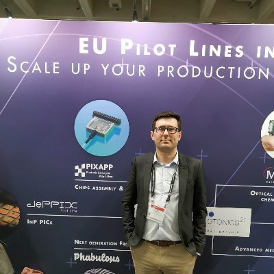
Looking forward to speaking about Photonics Packaging this morning at the 8th ePIXfab European Silicon Photonics Alliance #siliconphotonics summer school.


$GFS is the on-shore Foundry. Not great for $INTC: GlobalFoundries Announces $16B U.S. Investment to Reshore Essential Chip Manufacturing and Accelerate AI Growth Specifically calls out #SiliconPhotonics facility gf.com/gf-press-relea…

"Global Foundries Announces New York Advanced Packaging and Photonics Center" Did $GFS just become a play on #SiliconPhotonics? Advanced packaging equipment makers are going to benefit, as well: $BESI, $ASMPT, $KLIC globenewswire.com/news-release/2…


Full house in Copenhagen! 🙌 Over 130 joined our #SiliconPhotonics Workshop during #ECOC2025. Insights from @lightcounting , @ST_World , @Coherent, @nvidia on AI connectivity. Thanks to @eetimes for coverage. Hosted by @Soitec_Official & @CEA_Leti. #AI #Innovation


#ECIO2023 started yesterday at University of Twente! And of course, we couldn't miss it! We'll be presenting some of the results of the group on #SiliconPhotonics, be ready!


Visit us at @ECOC_Exhibition booth C4119! The blue suits are ready to discuss scalable, high-performance #photonics packaging: ★ PIC+RF up to 110 GHz ★ 3D-printed microlenses ★ LCP air cavity packages for volume manufacturing #meetthexperts #siliconphotonics #ECOC2025

Getting ready for #PhotonicsWest2023! What a best way to discover SF than a bike tour 🚴♀️ through the Golden Gate? And don't forget, you can see us all, and our recent works, during these next days. #SiliconPhotonics #MiNaPhot


The team are happy to be back at Laser World of Photonics @PHOTONICSWORLD They have a packed schedule but are having some fun along the way! #LASERworldofPhotonics #siliconphotonics


The STARLight consortium brings together leading industrial and academic partners in a project that aims to turn Europe into a technology leader in 300mm silicon photonics (SiPho) technology. newelectronics.co.uk/content/news/s… #SiliconPhotonics #300mmWaferTech #EuropeanInnovation
A new year starts, and here everything is getting ready for the first event of 2024: @PhotonicsWest! 🥳 Want to know more about our recent research on #siliconphotonics? Join us on🗓️29-31 January! See you there! 🤗


We are pleased to share that GF is attending #ECOC2025 in Copenhagen with two opportunities to explore the latest advancements to our #SiliconPhotonics platform for #CoPackagedOptics We look forward to connecting with those attending ECOC this week!

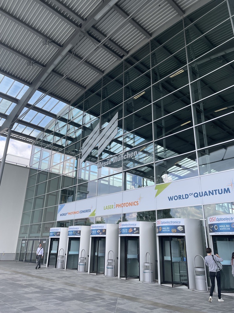
Some of us are attending this week the 8th @epixfab Silicon Photonics Summer School, at @ugent, @PhotonicsUGent ! 😄 #SiliconPhotonics @C2N_com


Join us for an online panel discussion organized by @electrooptics. During the webcast, Vincent Fraisse will highlight "ST optical interconnects technology roadmap: the role of #siliconphotonics technology in meeting increasing AI requirements". ➡️ spkl.io/6018ARcBA


The Cornerstone Photonics Innovation Centre (C-PIC), has launched a new Open Platform to facilitate open-source collaboration between academia and industry. eurekamagazine.co.uk/content/news/c… #SiliconPhotonics #OpenSourceInnovation #PhotonicsResearch #EurekaMagazine

Via #OPG_OpticaQ: Quantum teleportation of a silicon nanophotonic CNOT gate bit.ly/41WZSas #SiliconPhotonics #QuantumTeleportation @UCLA


Turn Your Research into Reality: #CORNERSTONE and Future Worlds Seek #Applicants for New #SiliconPhotonics Startup Stream #technologynews #electronicsnews #electronics #technology #technews #electronicsera #semiconductor #powerelectronics electronicsera.in/turn-your-rese…


✨ 𝗖𝘂𝘀𝘁𝗼𝗺 𝗦𝗶𝗹𝗶𝗰𝗼𝗻 𝗣𝗜𝗖𝘀? 𝗦𝗶𝗣𝗵𝗼𝘁𝗼𝗻𝗜𝗖 𝗱𝗲𝗹𝗶𝘃𝗲𝗿𝘀. 220/250nm SOI, custom stacks, novel processes. DUV, E-beam, maskless lithography options. Learn more: siphotonic.com Contact: [email protected] #SiliconPhotonics #NanoFabrication

Via #OPG_OMEx: MBE growth of GaSb on Ge-based templates grown on Si for mid-infrared photonics [Invited] bit.ly/430cD4z #EpitaxialIntegration #SiliconPhotonics @umontpellier
![OpticaPubsGroup's tweet image. Via #OPG_OMEx: MBE growth of GaSb on Ge-based templates grown on Si for mid-infrared photonics [Invited] bit.ly/430cD4z #EpitaxialIntegration #SiliconPhotonics @umontpellier](https://pbs.twimg.com/media/G4tj0R9W4AAwWC0.jpg)
An Editors' Pick via #OPG_OpEx: Compact and temperature-insensitive wavelength detectors integrated with widely tunable external-cavity lasers bit.ly/4qwq2eO #SiliconPhotonics #WavelengthDetectors @ShandongUni1901

Chip giant AMD is reportedly establishing two new research and development centers in Taiwan...ic-pcb.com/amd-280-millio… #AMD #SiliconPhotonics #CoPackagedOptics #HeterogeneousIntegration #AIChips #HighPerformanceComputing #DataCenterTech #AIHardware

🚀 𝗦𝗶𝗣𝗵𝗼𝘁𝗼𝗻𝗜𝗖'𝘀 𝗦𝗢𝗜 𝗣𝗹𝗮𝘁𝗳𝗼𝗿𝗺𝘀. Standard and Improved SOI with 220nm/250nm PDK libraries. Improved SOI offers <1dB coupling loss. Innovate with us! Learn more: siphotonic.com Contact: [email protected] #SiliconPhotonics #Innovation


The initiative connects #AIchips, compute centers, and photonic R&D into one integrated ecosystem — signaling that the next wave of AI innovation will run on light, not just silicon. #SiliconPhotonics #Photonics #Semiconductors #NVIDIA #TSMC ▶️Read more aistrategica.com/taiwans-ai-new…


Are you ready to dive into the cutting-edge world of #SiliconPhotonics? This groundbreaking technology is revolutionizing industries like autonomous driving, high-speed data communication, advanced sensors, and even life sciences! mycronic.com/product-areas/…


🏆 Wafer winners $TSEM Tower Semi & $TSM TSMC print the bigger Si-photonic dice that sit next to the switch chip. Fewer chips, but each is HUGE → wafer demand flat-to-UP. #SiliconPhotonics

@MarvellTech's Kishore Atreya demonstrates silicon photonics integration in their CPO switching platform. Key insight: scale-out test vehicles will lead, but real volume opportunities emerge in scale-up by decade's end ngi.fyi/ocp25-marvell-… #SiliconPhotonics

👀 #Siliconphotonics breakthrough! Columbia University researchers just showcased a high-power frequency comb light source on a chip — a big step toward compact CPO packages and next-gen optical transceivers!💡More: buff.ly/WaCRPAI 🔗


The next digital infrastructure revolution won’t be electronic… it will be photonic. The #SiliconPhotonics market is set to grow from $2.6B in 2025 to $9.6B by 2030 (29.5% CAGR). Investing now means backing the backbone of future #AI and #QuantumComputing.

Silicon Photonics – An Update from Prof. Keren Bergman on a Potentially Transformational Technology for Data Center Chips: @HPCpodcast wp.me/p3RLHQ-pkn @Columbia #opticalIO #siliconphotonics #interconnects #HPC #AI #AIdatacenter
#Duke of Edinburgh shines a light on #siliconphotonics during visit to C-PIC and University of Southampton #technologynews #electronicsnews #electronics #technology #technews #electronicsera #semiconductor #powerelectronics electronicsera.in/duke-of-edinbu…
electronicsera.in
Duke of Edinburgh shines a light on silicon photonics during visit to C-PIC and University of...
CORNERSTONE Photonics Innovation Centre (C-PIC), the UK’s dedicated Innovation and Knowledge Centre (IKC) for silicon photonics, was honoured to welcome
Scientists in Michal Lipson’s lab at Columbia University have achieved a breakthrough in silicon photonics frequency combs, creating high-power frequency combs on a single chip. eurekamagazine.co.uk/content/news/r… #SiliconPhotonics #FrequencyCombs #DataTransmissionInnovation
Full house in Copenhagen! 🙌 Over 130 joined our #SiliconPhotonics Workshop during #ECOC2025. Insights from @lightcounting , @ST_World , @Coherent, @nvidia on AI connectivity. Thanks to @eetimes for coverage. Hosted by @Soitec_Official & @CEA_Leti. #AI #Innovation

A chip smaller than a fingernail can now generate dozens of stable, high-power light wavelengths at once! A big win for efficiency in data centers... azooptics.com/News.aspx?news… #SiliconPhotonics #AZoOptics #DataCenters


#InnovativeTsinghua researchers proposed a reconfigurable #quantum entanglement distribution network using #siliconphotonics, reducing wavelength channels to O(N) and improving the scalability, reconfigurability, and performance of quantum technology. bit.ly/3W9PvNx

🌐 #TSMC は、#SiliconPhotonics 技術の成熟に伴い、今後の爆発的な成長を見込んでいると報じられています。SEMICON Taiwan では、銅–銅接合やハイブリッドボンディングを用いて、電子回路とフォトニック回路をウェハー上で接続する「COUPE」を発表しました。💡詳細:buff.ly/FPAlgKs 🔗

Via #OPG_OpticaQ: Quantum teleportation of a silicon nanophotonic CNOT gate bit.ly/41WZSas #SiliconPhotonics #QuantumTeleportation @UCLA
原來的目的是為了記錄自己的產業研究才創版 結果先做了記憶體報價XD 但一直發報價也很水(報價最近也很水) 所以最近會寫點矽光子的科普研究 什麼是矽光子? 1.簡單來說就是將光學系統,利用半導體製程微縮到晶片(PIC)上,並且利用光來傳遞訊號,實現低延遲、高容量、低功耗 #Siliconphotonics #矽光子
An Editors' Pick via #OPG_OpEx: In situ thermal trimming of waveguides in a standard active silicon photonics platform bit.ly/4nWCnap #SiliconPhotonics #ThermalAnnealing @mpi_msp

Broadband mode exchanger based on subwavelength Y-junctions #siliconphotonics #inversedesign degruyter.com/document/doi/1…

🌐 #TSMC reportedly expects explosive growth ahead for #SiliconPhotonics as the tech matures. At SEMICON Taiwan, it unveiled “COUPE,” linking electronic and photonic circuits on wafers with copper-to-copper bonding and hybrid bonding techniques.💡More: buff.ly/FPAlgKs 🔗
Join us for an online panel discussion organized by @electrooptics. During the webcast, Vincent Fraisse will highlight "ST optical interconnects technology roadmap: the role of #siliconphotonics technology in meeting increasing AI requirements". ➡️ spkl.io/6018ARcBA
Via #OPG_Optica: On-chip optical skyrmionic beam generators bit.ly/3ZzSM9Y #SiliconPhotonics #OrbitalAngularMomentum @sciencetokyo_ja

An Editors' Pick via #OPG_OL: Inverse-designed silicon nitride reflectors ow.ly/Ko4550QG6H2 #IntegratedOptics #SiliconPhotonics @etsmtl

Facilitating high-capacity optical communications and interconnects: Four-channel graphene optical receiver #siliconphotonics #photodetectors #opticalreceiver degruyter.com/document/doi/1…

Inverse-designed taper configuration for the enhancement of integrated 1 × 4 silicon photonic power splitters #siliconphotonics #photonicpowersplitter #particleswarmoptimization degruyter.com/document/doi/1…

For the latest research on #ThinFilmProcessing #FiberLasers and #SiliconPhotonics sign up for ToC alerts: marketing.degruyter.com/nanophotonics?…

We are pleased to share that GF is attending #ECOC2025 in Copenhagen with two opportunities to explore the latest advancements to our #SiliconPhotonics platform for #CoPackagedOptics We look forward to connecting with those attending ECOC this week!
We are willing and eager for femtosecond technology applications, but are photonic integrated circuits ready for this new paradigm? Read more: degruyter.com/document/doi/1… #ultrafastphotonics #siliconphotonics

Review: Towards large-scale programmable silicon photonic chip for signal processing #opticalsignalprocessing #siliconphotonics degruyter.com/document/doi/1…


Presented my masters research today at UBC ECE research day for the first time! Looking forward to publishing it soon. More info - gsa.ece.ubc.ca/research-day-2… #GradDiaries #SiliconPhotonics


We are proud to celebrate the remarkable achievements of Dr. @awanishpande, an alumnus of CeNSE, IISc, now a faculty @iitdelhi. His talk highlighted #siliconphotonics #sensors #ringresonators #applications His achievements in research continue to make the CeNSE community proud.


#ECIO2023 started yesterday at University of Twente! And of course, we couldn't miss it! We'll be presenting some of the results of the group on #SiliconPhotonics, be ready!
Via #OPG_Optica: 2D material platform for overcoming the amplitude–phase tradeoff in ring resonators ow.ly/etsZ50QAAIz #PhaseModulators #SiliconPhotonics @EE_ColumbiaSEAS

Something went wrong.
Something went wrong.
United States Trends
- 1. #WWERaw 70.1K posts
- 2. Packers 47.9K posts
- 3. Packers 47.9K posts
- 4. John Cena 67.2K posts
- 5. Jalen 16.1K posts
- 6. #GoPackGo 4,989 posts
- 7. Jordan Love 4,195 posts
- 8. #RawOnNetflix 1,737 posts
- 9. Grand Slam Champion 20.2K posts
- 10. Matt LaFleur 1,174 posts
- 11. Lane Johnson N/A
- 12. Cam Whitmore 1,058 posts
- 13. Kevin Patullo N/A
- 14. Green Bay 11.6K posts
- 15. Mailata N/A
- 16. #MondayNightFootball N/A
- 17. Rusev 2,901 posts
- 18. Tush Push 10.9K posts
- 19. Cade Horton 1,245 posts
- 20. Shipley N/A