#siliconphotonics search results
#InnovativeTsinghua researchers proposed a reconfigurable #quantum entanglement distribution network using #siliconphotonics, reducing wavelength channels to O(N) and improving the scalability, reconfigurability, and performance of quantum technology. bit.ly/3W9PvNx

原來的目的是為了記錄自己的產業研究才創版 結果先做了記憶體報價XD 但一直發報價也很水(報價最近也很水) 所以最近會寫點矽光子的科普研究 什麼是矽光子? 1.簡單來說就是將光學系統,利用半導體製程微縮到晶片(PIC)上,並且利用光來傳遞訊號,實現低延遲、高容量、低功耗 #Siliconphotonics #矽光子

🌐 #TSMC reportedly expects explosive growth ahead for #SiliconPhotonics as the tech matures. At SEMICON Taiwan, it unveiled “COUPE,” linking electronic and photonic circuits on wafers with copper-to-copper bonding and hybrid bonding techniques.💡More: buff.ly/FPAlgKs 🔗

NVIDIA #SiliconPhotonics is powering the next leap in AI networking: ✅ 3.5× better power efficiency ✅ 10× higher resiliency ✅ 1.3× faster deployment Co-Packaged Optics-Based networks simplify design, free more power for compute, and scale to million-GPU AI factories. 👉…
Looking forward to speaking about Photonics Packaging this morning at the 8th ePIXfab European Silicon Photonics Alliance #siliconphotonics summer school.

$GFS is the on-shore Foundry. Not great for $INTC: GlobalFoundries Announces $16B U.S. Investment to Reshore Essential Chip Manufacturing and Accelerate AI Growth Specifically calls out #SiliconPhotonics facility gf.com/gf-press-relea…

"Global Foundries Announces New York Advanced Packaging and Photonics Center" Did $GFS just become a play on #SiliconPhotonics? Advanced packaging equipment makers are going to benefit, as well: $BESI, $ASMPT, $KLIC globenewswire.com/news-release/2…

#ECIO2023 started yesterday at University of Twente! And of course, we couldn't miss it! We'll be presenting some of the results of the group on #SiliconPhotonics, be ready!

Full house in Copenhagen! 🙌 Over 130 joined our #SiliconPhotonics Workshop during #ECOC2025. Insights from @lightcounting , @ST_World , @Coherent, @nvidia on AI connectivity. Thanks to @eetimes for coverage. Hosted by @Soitec_Official & @CEA_Leti. #AI #Innovation

Visit us at @ECOC_Exhibition booth C4119! The blue suits are ready to discuss scalable, high-performance #photonics packaging: ★ PIC+RF up to 110 GHz ★ 3D-printed microlenses ★ LCP air cavity packages for volume manufacturing #meetthexperts #siliconphotonics #ECOC2025

The team are happy to be back at Laser World of Photonics @PHOTONICSWORLD They have a packed schedule but are having some fun along the way! #LASERworldofPhotonics #siliconphotonics


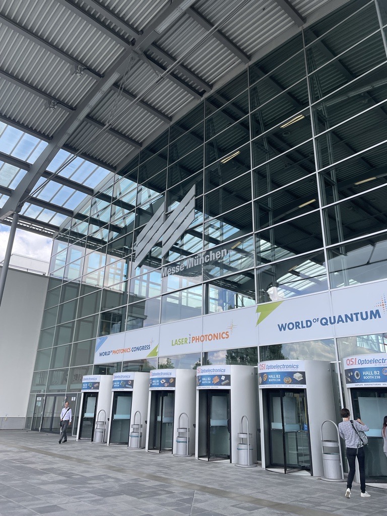
Getting ready for #PhotonicsWest2023! What a best way to discover SF than a bike tour 🚴♀️ through the Golden Gate? And don't forget, you can see us all, and our recent works, during these next days. #SiliconPhotonics #MiNaPhot

We are pleased to share that GF is attending #ECOC2025 in Copenhagen with two opportunities to explore the latest advancements to our #SiliconPhotonics platform for #CoPackagedOptics We look forward to connecting with those attending ECOC this week!

The STARLight consortium brings together leading industrial and academic partners in a project that aims to turn Europe into a technology leader in 300mm silicon photonics (SiPho) technology. newelectronics.co.uk/content/news/s… #SiliconPhotonics #300mmWaferTech #EuropeanInnovation
Some of us are attending this week the 8th @epixfab Silicon Photonics Summer School, at @ugent, @PhotonicsUGent ! 😄 #SiliconPhotonics @C2N_com

A new year starts, and here everything is getting ready for the first event of 2024: @PhotonicsWest! 🥳 Want to know more about our recent research on #siliconphotonics? Join us on🗓️29-31 January! See you there! 🤗

Join GF in the #OFC2025 technical sessions to hear the latest advancements in #SiliconPhotonics that can be integrated onto our monolithic GF Fotonix platform for even more design flexibility to enable your next-generation PICs!

GF will be onsite at #OFC2025 this year, showcasing our latest #SiliconPhotonics advancements to our GF Fotonix platform! Visit Booth 3220 to speak with our technical experts and browse GF Fotonix chiplet designs from our customers & partners. We look forward to seeing you there!

Join us for an online panel discussion organized by @electrooptics. During the webcast, Vincent Fraisse will highlight "ST optical interconnects technology roadmap: the role of #siliconphotonics technology in meeting increasing AI requirements". ➡️ spkl.io/6018ARcBA

Turn Your Research into Reality: #CORNERSTONE and Future Worlds Seek #Applicants for New #SiliconPhotonics Startup Stream #technologynews #electronicsnews #electronics #technology #technews #electronicsera #semiconductor #powerelectronics electronicsera.in/turn-your-rese…

✨ 𝗖𝘂𝘀𝘁𝗼𝗺 𝗦𝗶𝗹𝗶𝗰𝗼𝗻 𝗣𝗜𝗖𝘀? 𝗦𝗶𝗣𝗵𝗼𝘁𝗼𝗻𝗜𝗖 𝗱𝗲𝗹𝗶𝘃𝗲𝗿𝘀. 220/250nm SOI, custom stacks, novel processes. DUV, E-beam, maskless lithography options. Learn more: siphotonic.com Contact: [email protected] #SiliconPhotonics #NanoFabrication

Via #OPG_OMEx: MBE growth of GaSb on Ge-based templates grown on Si for mid-infrared photonics [Invited] bit.ly/430cD4z #EpitaxialIntegration #SiliconPhotonics @umontpellier
![OpticaPubsGroup's tweet image. Via #OPG_OMEx: MBE growth of GaSb on Ge-based templates grown on Si for mid-infrared photonics [Invited] bit.ly/430cD4z #EpitaxialIntegration #SiliconPhotonics @umontpellier](https://pbs.twimg.com/media/G4tj0R9W4AAwWC0.jpg)
An Editors' Pick via #OPG_OpEx: Compact and temperature-insensitive wavelength detectors integrated with widely tunable external-cavity lasers bit.ly/4qwq2eO #SiliconPhotonics #WavelengthDetectors @ShandongUni1901

Chip giant AMD is reportedly establishing two new research and development centers in Taiwan...ic-pcb.com/amd-280-millio… #AMD #SiliconPhotonics #CoPackagedOptics #HeterogeneousIntegration #AIChips #HighPerformanceComputing #DataCenterTech #AIHardware

🚀 𝗦𝗶𝗣𝗵𝗼𝘁𝗼𝗻𝗜𝗖'𝘀 𝗦𝗢𝗜 𝗣𝗹𝗮𝘁𝗳𝗼𝗿𝗺𝘀. Standard and Improved SOI with 220nm/250nm PDK libraries. Improved SOI offers <1dB coupling loss. Innovate with us! Learn more: siphotonic.com Contact: [email protected] #SiliconPhotonics #Innovation

The initiative connects #AIchips, compute centers, and photonic R&D into one integrated ecosystem — signaling that the next wave of AI innovation will run on light, not just silicon. #SiliconPhotonics #Photonics #Semiconductors #NVIDIA #TSMC ▶️Read more aistrategica.com/taiwans-ai-new…

Are you ready to dive into the cutting-edge world of #SiliconPhotonics? This groundbreaking technology is revolutionizing industries like autonomous driving, high-speed data communication, advanced sensors, and even life sciences! mycronic.com/product-areas/…

🏆 Wafer winners $TSEM Tower Semi & $TSM TSMC print the bigger Si-photonic dice that sit next to the switch chip. Fewer chips, but each is HUGE → wafer demand flat-to-UP. #SiliconPhotonics
@MarvellTech's Kishore Atreya demonstrates silicon photonics integration in their CPO switching platform. Key insight: scale-out test vehicles will lead, but real volume opportunities emerge in scale-up by decade's end ngi.fyi/ocp25-marvell-… #SiliconPhotonics

👀 #Siliconphotonics breakthrough! Columbia University researchers just showcased a high-power frequency comb light source on a chip — a big step toward compact CPO packages and next-gen optical transceivers!💡More: buff.ly/WaCRPAI 🔗
The next digital infrastructure revolution won’t be electronic… it will be photonic. The #SiliconPhotonics market is set to grow from $2.6B in 2025 to $9.6B by 2030 (29.5% CAGR). Investing now means backing the backbone of future #AI and #QuantumComputing.
Silicon Photonics – An Update from Prof. Keren Bergman on a Potentially Transformational Technology for Data Center Chips: @HPCpodcast wp.me/p3RLHQ-pkn @Columbia #opticalIO #siliconphotonics #interconnects #HPC #AI #AIdatacenter
#Duke of Edinburgh shines a light on #siliconphotonics during visit to C-PIC and University of Southampton #technologynews #electronicsnews #electronics #technology #technews #electronicsera #semiconductor #powerelectronics electronicsera.in/duke-of-edinbu…
electronicsera.in
Duke of Edinburgh shines a light on silicon photonics during visit to C-PIC and University of...
CORNERSTONE Photonics Innovation Centre (C-PIC), the UK’s dedicated Innovation and Knowledge Centre (IKC) for silicon photonics, was honoured to welcome
Scientists in Michal Lipson’s lab at Columbia University have achieved a breakthrough in silicon photonics frequency combs, creating high-power frequency combs on a single chip. eurekamagazine.co.uk/content/news/r… #SiliconPhotonics #FrequencyCombs #DataTransmissionInnovation
Full house in Copenhagen! 🙌 Over 130 joined our #SiliconPhotonics Workshop during #ECOC2025. Insights from @lightcounting , @ST_World , @Coherent, @nvidia on AI connectivity. Thanks to @eetimes for coverage. Hosted by @Soitec_Official & @CEA_Leti. #AI #Innovation

A chip smaller than a fingernail can now generate dozens of stable, high-power light wavelengths at once! A big win for efficiency in data centers... azooptics.com/News.aspx?news… #SiliconPhotonics #AZoOptics #DataCenters

#InnovativeTsinghua researchers proposed a reconfigurable #quantum entanglement distribution network using #siliconphotonics, reducing wavelength channels to O(N) and improving the scalability, reconfigurability, and performance of quantum technology. bit.ly/3W9PvNx

🌐 #TSMC は、#SiliconPhotonics 技術の成熟に伴い、今後の爆発的な成長を見込んでいると報じられています。SEMICON Taiwan では、銅–銅接合やハイブリッドボンディングを用いて、電子回路とフォトニック回路をウェハー上で接続する「COUPE」を発表しました。💡詳細:buff.ly/FPAlgKs 🔗

🌐 #TSMC reportedly expects explosive growth ahead for #SiliconPhotonics as the tech matures. At SEMICON Taiwan, it unveiled “COUPE,” linking electronic and photonic circuits on wafers with copper-to-copper bonding and hybrid bonding techniques.💡More: buff.ly/FPAlgKs 🔗

Via #OPG_OpticaQ: Quantum teleportation of a silicon nanophotonic CNOT gate bit.ly/41WZSas #SiliconPhotonics #QuantumTeleportation @UCLA

Broadband mode exchanger based on subwavelength Y-junctions #siliconphotonics #inversedesign degruyter.com/document/doi/1…

An Editors' Pick via #OPG_OpEx: In situ thermal trimming of waveguides in a standard active silicon photonics platform bit.ly/4nWCnap #SiliconPhotonics #ThermalAnnealing @mpi_msp

Facilitating high-capacity optical communications and interconnects: Four-channel graphene optical receiver #siliconphotonics #photodetectors #opticalreceiver degruyter.com/document/doi/1…

Presented my masters research today at UBC ECE research day for the first time! Looking forward to publishing it soon. More info - gsa.ece.ubc.ca/research-day-2… #GradDiaries #SiliconPhotonics


Via #OPG_Optica: On-chip optical skyrmionic beam generators bit.ly/3ZzSM9Y #SiliconPhotonics #OrbitalAngularMomentum @sciencetokyo_ja

Inverse-designed taper configuration for the enhancement of integrated 1 × 4 silicon photonic power splitters #siliconphotonics #photonicpowersplitter #particleswarmoptimization degruyter.com/document/doi/1…

原來的目的是為了記錄自己的產業研究才創版 結果先做了記憶體報價XD 但一直發報價也很水(報價最近也很水) 所以最近會寫點矽光子的科普研究 什麼是矽光子? 1.簡單來說就是將光學系統,利用半導體製程微縮到晶片(PIC)上,並且利用光來傳遞訊號,實現低延遲、高容量、低功耗 #Siliconphotonics #矽光子

An Editors' Pick via #OPG_OL: Inverse-designed silicon nitride reflectors ow.ly/Ko4550QG6H2 #IntegratedOptics #SiliconPhotonics @etsmtl

We are willing and eager for femtosecond technology applications, but are photonic integrated circuits ready for this new paradigm? Read more: degruyter.com/document/doi/1… #ultrafastphotonics #siliconphotonics

Join us for an online panel discussion organized by @electrooptics. During the webcast, Vincent Fraisse will highlight "ST optical interconnects technology roadmap: the role of #siliconphotonics technology in meeting increasing AI requirements". ➡️ spkl.io/6018ARcBA

For the latest research on #ThinFilmProcessing #FiberLasers and #SiliconPhotonics sign up for ToC alerts: marketing.degruyter.com/nanophotonics?…

Review: Towards large-scale programmable silicon photonic chip for signal processing #opticalsignalprocessing #siliconphotonics degruyter.com/document/doi/1…

#ECIO2023 started yesterday at University of Twente! And of course, we couldn't miss it! We'll be presenting some of the results of the group on #SiliconPhotonics, be ready!

We are proud to celebrate the remarkable achievements of Dr. @awanishpande, an alumnus of CeNSE, IISc, now a faculty @iitdelhi. His talk highlighted #siliconphotonics #sensors #ringresonators #applications His achievements in research continue to make the CeNSE community proud.


Congrats to the authors of 'Reconfigurable application-specific photonic integrated circuit for solving partial differential equations' whose research is already gathering citations. #photonics #siliconphotonics degruyter.com/document/doi/1…


Looking forward to speaking about Photonics Packaging this morning at the 8th ePIXfab European Silicon Photonics Alliance #siliconphotonics summer school.

Something went wrong.
Something went wrong.
United States Trends
- 1. Daboll 36.1K posts
- 2. Pond 238K posts
- 3. Schoen 18.6K posts
- 4. Schoen 18.6K posts
- 5. Veterans Day 21.3K posts
- 6. Joe Burrow 5,637 posts
- 7. Giants 71.8K posts
- 8. Go Birds 11.5K posts
- 9. Dart 23.2K posts
- 10. Kim Davis 12.7K posts
- 11. #ROBOGIVE 1,065 posts
- 12. Marines 61.1K posts
- 13. Joe Dirt N/A
- 14. Zendaya 8,034 posts
- 15. #jimromeonx N/A
- 16. Jeffries 40.7K posts
- 17. Johnny Carson N/A
- 18. Hanoi Jane N/A
- 19. Semper Fi 11.7K posts
- 20. Edmund Fitzgerald 10.1K posts


